Fully depleted SOI multiple threshold voltage application

a technology of multiple threshold voltage and soi, applied in the field of fully depleted soi multiple threshold voltage application, can solve the problems of significant devices, increased concern for leakage current, and body-tied methods may suffer from area and speed penalties

Active Publication Date: 2005-11-03
TAIWAN SEMICON MFG CO LTD
View PDF10 Cites 50 Cited by
  • Summary
  • Abstract
  • Description
  • Claims
  • Application Information

AI Technical Summary

Benefits of technology

[0014] In accordance with another illustrative embodiment of the present invention, a semiconductor chip comprises a substrate. The substrate comprises at least one buried dielectric, the buried dielectric having a first buried dielectric thickness in a first Vth region greater than a second buried dielectric thickness in a second Vth region, wherein the difference between the first Vth and the second Vth is about 0.15˜0.45 eV. Specific examples would include a core region having a Vth of about 0.2 eV (less than 1.8 eV) and an I / O region having a Vth of about 0.65 eV, wherein the barrier dielectric thickness of the core region is greater than the barrier dielectric thickness of the I / O region. For other applications, the threshold voltage of the I / O region may be greater than 1.8 eV.

Problems solved by technology

An existing challenge in SOI technology, however, is forming thin Si channel SOI I / O devices with significant voltage threshold (Vth) control.
Further, the higher voltages typically applied in the I / O regions increase the concern regarding leakage current.
However, despite reducing the floating body effect (FBE) in SOI devices, the body-tied method may suffer from area and speed penalties.
In addition, the benefits obtained by the body-tied method may diminish as SOI silicon thicknesses scale downward because the increasing body resistance will make the body contact useless.
Despite raising the Vth, however, channel implants reduce the depletion ability of an SOI device, thereby incurring performance degradation from the FBE.
It is difficult, however, to apply different gate work function materials for SOI core applications and I / O device applications on the same chip, for example.
However, for a fully-depleted SOI device, the threshold voltage cannot be adjusted by the channel or pocket implantation because heavy substrate concentration will turn the FD device into a partially depleted device and degrade the performance.

Method used


Image

  • Fully depleted SOI multiple threshold voltage application
  • Fully depleted SOI multiple threshold voltage application
  • Fully depleted SOI multiple threshold voltage application

Examples


Embodiment Construction

[0023] The making and using of the presently preferred embodiments are discussed in detail below. It should be appreciated, however, that the present invention provides many applicable inventive concepts that can be embodied in a wide variety of specific contexts. The specific embodiments discussed are merely illustrative of specific ways to make and use the invention, and do not limit the scope of the invention.

[0024] The present invention will be described with respect to preferred embodiments in a specific context, namely a fully depleted SOI multiple threshold voltage application. The invention may also be applied, however, to other semiconductor devices and semiconductor applications having a need for multiple threshold voltages on the same substrate.

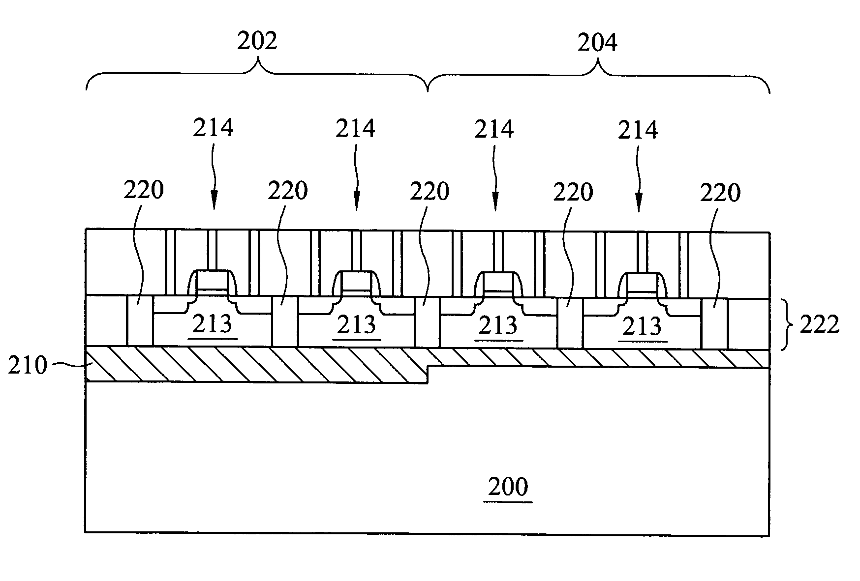
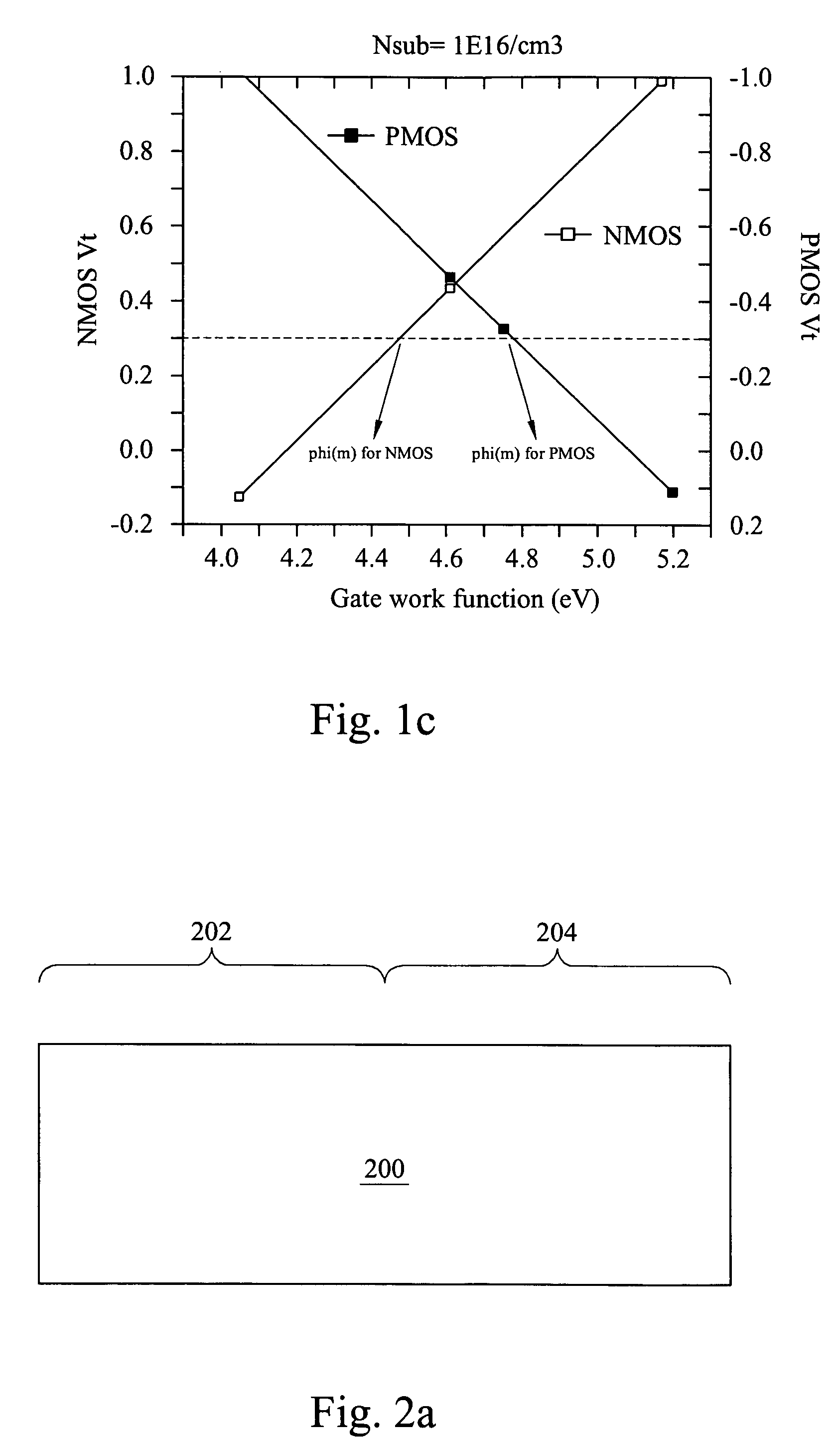
[0025] A substrate 200, shown in FIG. 2a, comprises a semiconductor substrate material. The substrate material is preferably a p-type doped substantially crystalline silicon material with a crystal orientation of . Alternatively,...


PUM


Abstract

An integrated circuit comprises a substrate and a buried dielectric formed in the substrate. The buried dielectric has a first thickness in a first region, a second buried dielectric thickness in a second region, and a step between the first and second regions. A semiconductor layer overlies the buried dielectric.

Description

[0001] This application claims the benefit of U.S. Provisional Application No. 60 / 566,040, filed on Apr. 28, 2004, entitled Fully Depleted SOI Multiple Threshold Voltage Application, which application is hereby incorporated herein by reference.TECHNICAL FIELD [0002] The present invention relates generally to semiconductor devices, and more particularly to a system and method for a fully depleted SOI multiple threshold voltage application. BACKGROUND [0003] In order to produce competitive electronic devices, it is often desired to produce semiconductor chips with several different regions (e.g., core region, low power region, I / O region) having semiconductor devices that vary according to speed and power, for example. Semiconductor devices that provide some or all of these features include silicon-on-insulator (SOI) devices. An existing challenge in SOI technology, however, is forming thin Si channel SOI I / O devices with significant voltage threshold (Vth) control. For example, in an...

Claims


Application Information

Patent Timeline
Patent Type & Authority Applications(United States)
IPC IPC(8): H01L21/762H01L21/84H01L27/12H01L29/786
CPCH01L21/76267H01L21/76283H01L29/78603H01L27/1203H01L21/84
Inventor CHEN, HAO-YUCHANG, CHANG-YUNLEE, DI-HONGYANG, FU-LIANG
Owner TAIWAN SEMICON MFG CO LTD
Why Eureka
Try Eureka