Field emission display

a field emission display and field emission technology, applied in the field of field emission display, can solve the problems of high cost of drive circuit of high voltage, inability to implement low voltage drive, and inability to control electron emission control and driving voltage of field emission, etc., to achieve enhanced fed brightness, the effect of facilitating the manufacturing process and high voltag

Active Publication Date: 2005-11-10
ELECTRONICS & TELECOMM RES INST
View PDF8 Cites 36 Cited by
  • Summary
  • Abstract
  • Description
  • Claims
  • Application Information

AI Technical Summary

Benefits of technology

[0021] The present invention is also directed to an FED configured to apply an electric field required for field emission via a gate electrode to allow an interval between an anode portion and a cathode portion to be freely adjusted so that a high voltage may be applied to the anode electrode and resultant b

Problems solved by technology

As compared with the triode type field emission device, the diode type field emission device has advantages that its manufacturing process is simple and the reliability of electron emission is good, however, has disadvantages in terms of electron emission control and driving voltage of field emission.
In the FED having the diode type field emission device of FIG. 1, a high electric field required for the field emission (typically several V/um) is applied between the electrodes (cathode electrodes 11 and transparent anode electrodes 13 of FIG. 1) of both of the top and bottom substrates spaced apart from each other by a relatively long interval (typically ranged from 200 μm to 2 mm), so that a display signal should hav

Method used


Image

  • Field emission display
  • Field emission display
  • Field emission display

Examples


Embodiment Construction

[0036] The present invention will now be described more fully hereinafter with reference to the accompanying drawings, in which preferred embodiments of the invention are shown. This invention may, however, be embodied in different forms and should not be construed as limited to the embodiments set forth herein. Rather, these embodiments are provided so that this disclosure is thorough and complete and fully conveys the scope of the invention to those skilled in the art.

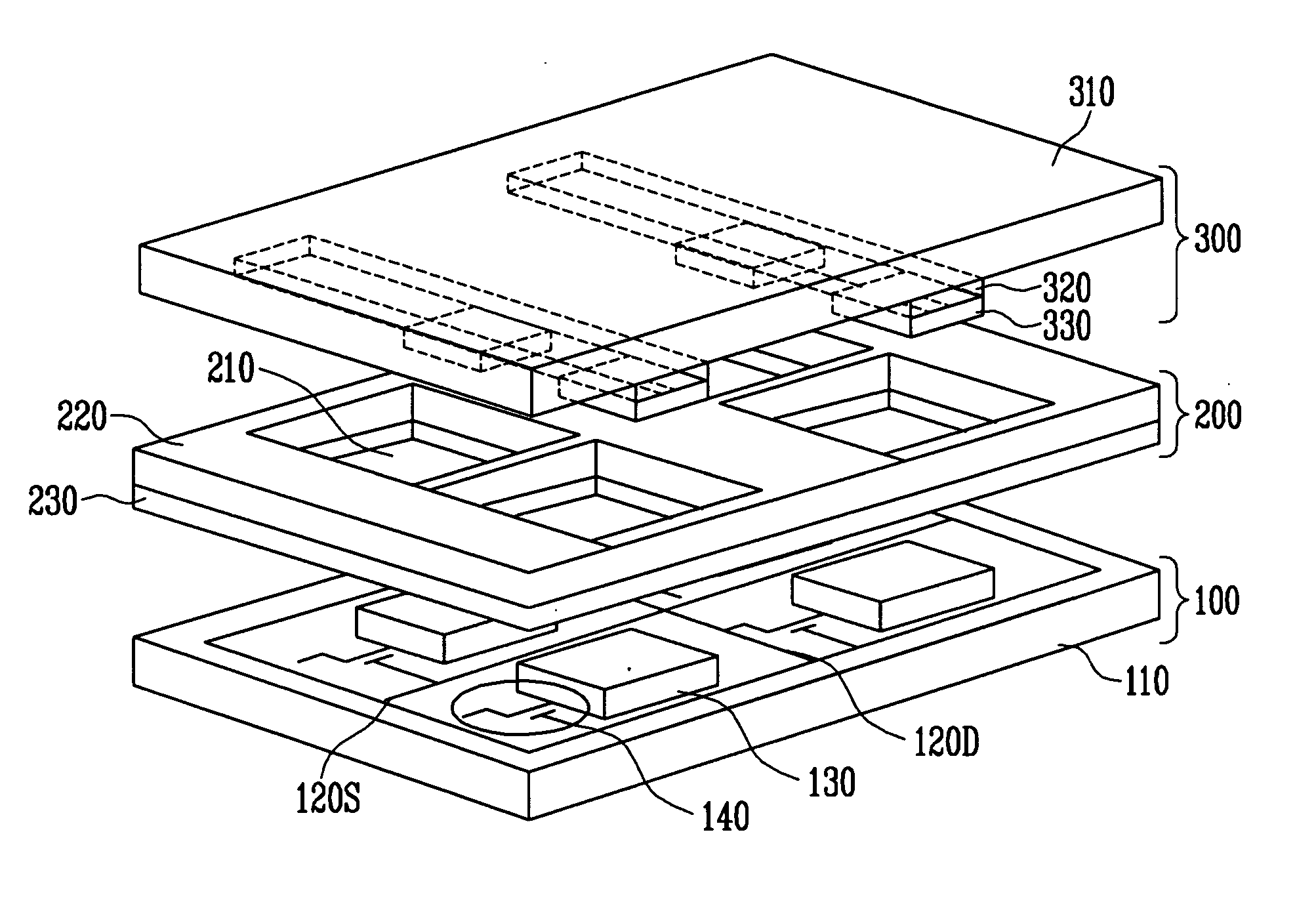
[0037]FIG. 3 is a schematic view illustrating a configuration of an FED in accordance with an embodiment of the present invention, and FIG. 4 is a schematic cross-sectional view of the FED of FIG. 3.

[0038] The FED of FIG. 3 is comprised of a cathode portion 100, a gate portion 200, and an anode portion 300.

[0039] The cathode portion 100 has a row signal line 120S and a column signal line 120D in a stripe form which are formed of conductive layers on a substrate 110 such as glass, plastic, various ceramics, various...


PUM


Abstract

Provided is a field emission display, which includes: a cathode portion including row signal lines and column signal lines in a stripe form allowing matrix addressing to be carried out on a substrate, and pixels defined by the row signal lines and the column signal lines, each pixel having a field emitter and a control device which controls the field emitter with two terminals connected to at least the row signal line and the column signal line and one terminal connected to the field emitter; an anode portion having an anode electrode, and a phosphor connected to the anode electrode; and a gate portion having a metal mesh with a plurality of penetrating holes, and a dielectric layer formed on at least one region of the metal mesh, wherein the gate portion is disposed between the cathode portion and the anode portion to allow the surface where the dielectric layer is formed to be faced to the cathode portion and to allow electrons emitted from the field emitter to collide with the phosphor via the penetrating holes.

Description

CROSS-REFERENCE TO RELATED APPLICATION [0001] This application claims priority to and the benefit of Korean Patent Application No. 2004-0031508,filed May 4, 2004,the disclosure of which is incorporated herein by reference in its entirety. BACKGROUND [0002] 1. Field of the Invention [0003] The present invention relates to a field emission display (FED), and more particularly, to a field emission display comprising a gate portion, a cathode portion, and an anode portion, in which the gate portion is provided with a metal mesh and a dielectric layer formed on at least one region of the metal mesh. [0004] 2. Discussion of Related Art [0005] The FED comprises a cathode portion having a field emitter and an anode portion having a phosphor, which are opposite to and spaced apart from each other by a predetermined interval (e.g. 2 mm) and packaged in vacuum. In the FED, electrons are emitted from the field emitter of the cathode and collide with the phosphor of the anode, thereby displaying...

Claims


Application Information

Patent Timeline
IPC IPC(8): H01J1/30H01J1/304H01J29/04H01J29/06H01J31/12H05B44/00
CPCH01J31/127H01J29/06H01J1/304
Inventor SONG, YOON HOLEE, JIN HOHWANG, CHI SUN
Owner ELECTRONICS & TELECOMM RES INST
Why Eureka
Try Eureka