Method for generating timing constraints of logic circuit

Inactive Publication Date: 2005-11-10
SOCIONEXT INC
View PDF10 Cites 7 Cited by
  • Summary
  • Abstract
  • Description
  • Claims
  • Application Information

AI Technical Summary

Benefits of technology

[0015] It is therefore an object of the present invention to generate a timing constraint on a higher-level block without an error even when interface specifications of existing timing constrai

Problems solved by technology

With recent miniaturization in semiconductor fabrication processes, logic circuits to be designed have become larger in scale and more complicated.
Accordingly, if a timing constraint on a higher-level block is generated based on timing constraints on a plurality of lower-level blocks exhibiting no matching, the timing constraint on the higher-l

Method used


Image

  • Method for generating timing constraints of logic circuit
  • Method for generating timing constraints of logic circuit
  • Method for generating timing constraints of logic circuit

Examples


Example

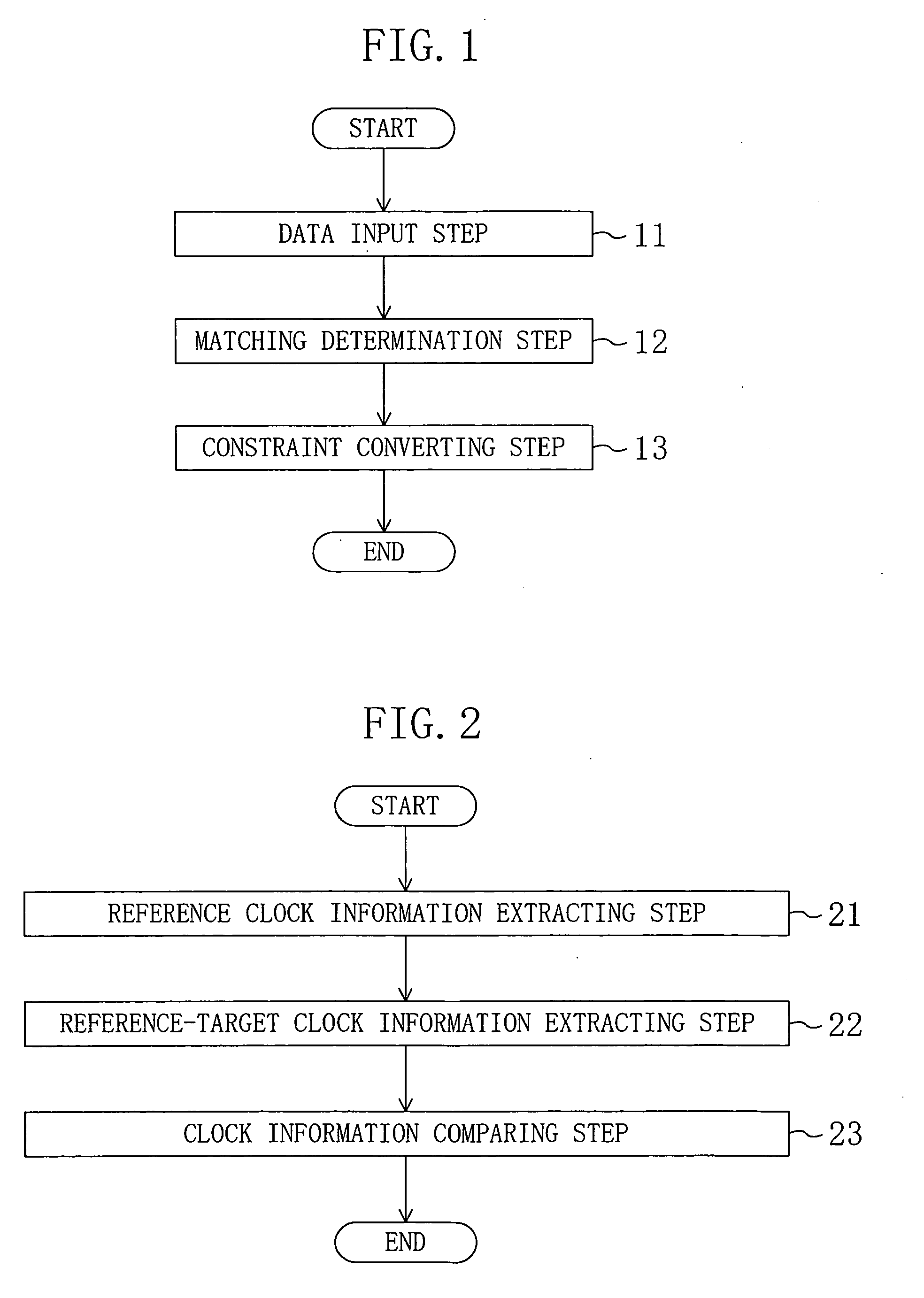
[0057] First, a first embodiment of the present invention will be described with reference to FIGS. 1, 2 and 8.

[0058]FIG. 1 is a flowchart showing process steps according to the first embodiment. In FIG. 1, step 11 is a data input step of inputting data on a logic circuit having a hierarchical structure, library data holding primitive information on the logic circuit and timing constraints on a plurality of circuit blocks at one or more lower levels of the logic circuit. Step 12 is a matching determination step of determining whether or not interface specifications of timing constraints on the lower-level blocks match each other based on the data that has been input at the data input step 11. Step 13 is a constraint converting step of converting timing constraints on the lower-level blocks after the matching determination into at least one constraint on a higher-level block. FIG. 1 for this embodiment is different from FIG. 4 for the conventional example in that the matching determ...

Example

[0066] Now, a second embodiment of the present invention will be described with reference to FIGS. 8, 9 and 10.

[0067]FIG. 9 is a flowchart showing process steps according to the second embodiment. The second embodiment is different from the first embodiment in that a matching determination step 12A of determining whether or not interface specifications match each other by comparing timing exception information (timing constraints) for changing timings of lower-level blocks to be connected to each other is provided instead of the matching determination step 12 of determining whether or not interface specifications match each other by comparing reference clock information. In this embodiment, the same reference numeral denotes the same component.

[0068]FIG. 10 shows the matching determination step 12A in detail. In FIG. 10, step 101 is a timing exception information extracting step of extracting timing exception information which has been set at an input pin or an output pin of a low...

Example

[0074] Now, a third embodiment of the present invention will be described with reference to FIGS. 11, 12, 13 and 14.

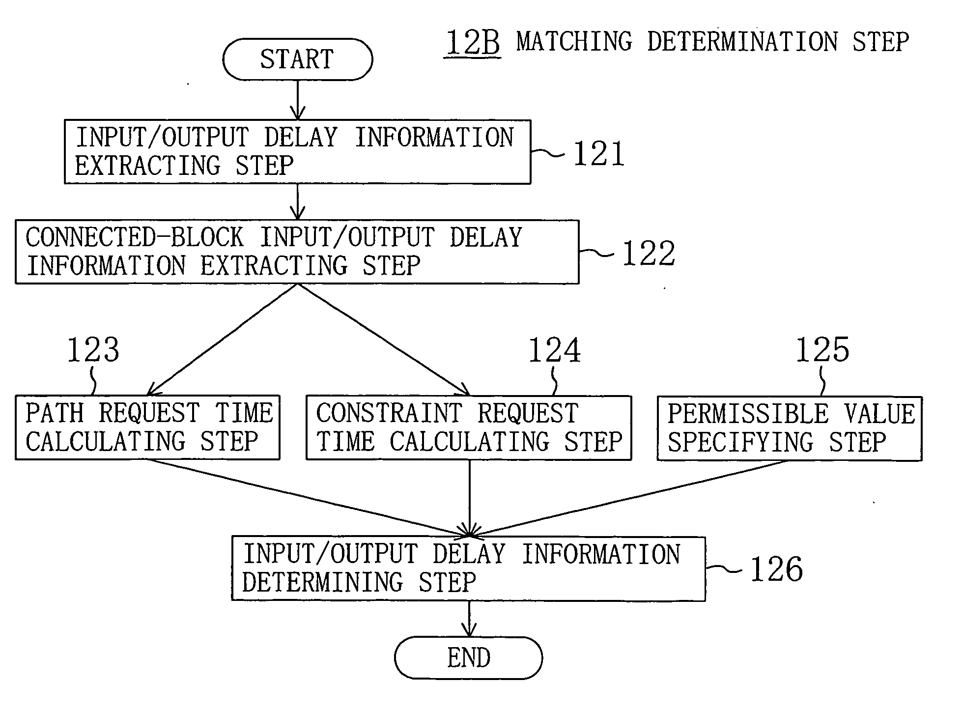
[0075]FIG. 11 shows a timing constraint generating method according to the third embodiment. The third embodiment shown in FIG. 11 is different from the first embodiment shown in FIG. 1 in that a matching determination step 12B of determining whether or not interface specifications match each other by determining the validity of input / output delay information is provided instead of the matching determination step 12 of determining whether or not interface specifications match each other by comparing reference clock information with each other. The input / output delay information is an output delay constraint as an external constraint on an output pin or an input delay constraint as an external constraint on an input pin.

[0076]FIG. 12 is a flowchart showing process steps of the matching determination step 12B shown in FIG. 11. Step 121 is an input / output delay informat...


PUM


Abstract

In hierarchical design of a logic circuit by utilizing lower-level blocks of the logic circuit, data on the logic circuit with the hierarchical structure, library data holding primitive information on the logic circuit and timing constraints on the lower-level blocks are input at a data input step. Based on these input data, it is determined whether or not interface specifications of timing constraints on the lower-level blocks match each other at a matching determination step before a constraint converting step of converting the timing constraints on the lower-level blocks into a timing constraint on a higher-level block. Accordingly, it is possible to avoid generation of an excessively reduced or rigorous timing constraint on the higher-level block resulting from mismatching between interface specifications of timing constraints on the lower-level blocks.

Description

CROSS-REFERENCE TO RELATED APPLICATION [0001] This Non-provisional application claims priority under 35 U.S.C. § 119(a) on Patent Application No. 2004-138916 filed in Japan on May 7, 2004, the entire contents of which are hereby incorporated by reference. BACKGROUND OF THE INVENTION [0002] The present invention relates to methods for generating timing constraints of logic circuits and particularly to a method for generating a timing constraint on a higher-level block in hierarchical design without an error. [0003] With recent miniaturization in semiconductor fabrication processes, logic circuits to be designed have become larger in scale and more complicated. Therefore, hierarchical design in which a logic circuit to be implemented is divided into a plurality of partial circuits each having a specific function and the partial circuits are designed in parallel has been adopted in most cases. [0004]FIG. 3 illustrates an example of a hierarchically designed logic circuit. A highest-lev...

Claims


Application Information

Patent Timeline
IPC IPC(8): G06F17/50
CPCG06F17/5045G06F17/5031G06F30/3312G06F30/30G06F2119/12
Inventor NAKASHIBA, TAKAFUMI
Owner SOCIONEXT INC
Why Eureka
Try Eureka