Electron emission display (EED) with separated grounds

a technology of electron emission display and separated ground, which is applied in the field of electron emission display with separated ground, can solve the problems of rf noise having a bad influence on the mutual influence of rf noise, affecting the performance of rf noise, and increasing rf noise as much, so as to reduce the influence of nois

Inactive Publication Date: 2005-11-17
SAMSUNG SDI CO LTD
View PDF4 Cites 6 Cited by
  • Summary
  • Abstract
  • Description
  • Claims
  • Application Information

AI Technical Summary

Benefits of technology

[0014] The present invention provides an EED which is capable of reducing noise influence transferred between a high voltage element and a low voltage element through a ground.

Problems solved by technology

Therefore, when a high voltage element and a low voltage element make use of a common ground, RF noise generated by the high voltage element is transferred to the low voltage element through the ground, causing an error in the low voltage element, for example, a logic circuit.
Thus, RF noise has a bad influence upon them mutually.
Specifically, as a frequency of a high voltage pulse supplied to the drivers increases, RF noise increases as much.
Since the high voltage elements are driven at an RF high voltage, noise occurs therein.
The noise influences the low voltage elements through the ground.
Also, RF noise occurring in the high voltage element can influence other digital logic elements through the ground.
Thus, the EED has a problem in that the picture quality of the images displayed on the EED panel is degraded.

Method used


Image

  • Electron emission display (EED) with separated grounds
  • Electron emission display (EED) with separated grounds
  • Electron emission display (EED) with separated grounds

Examples


Embodiment Construction

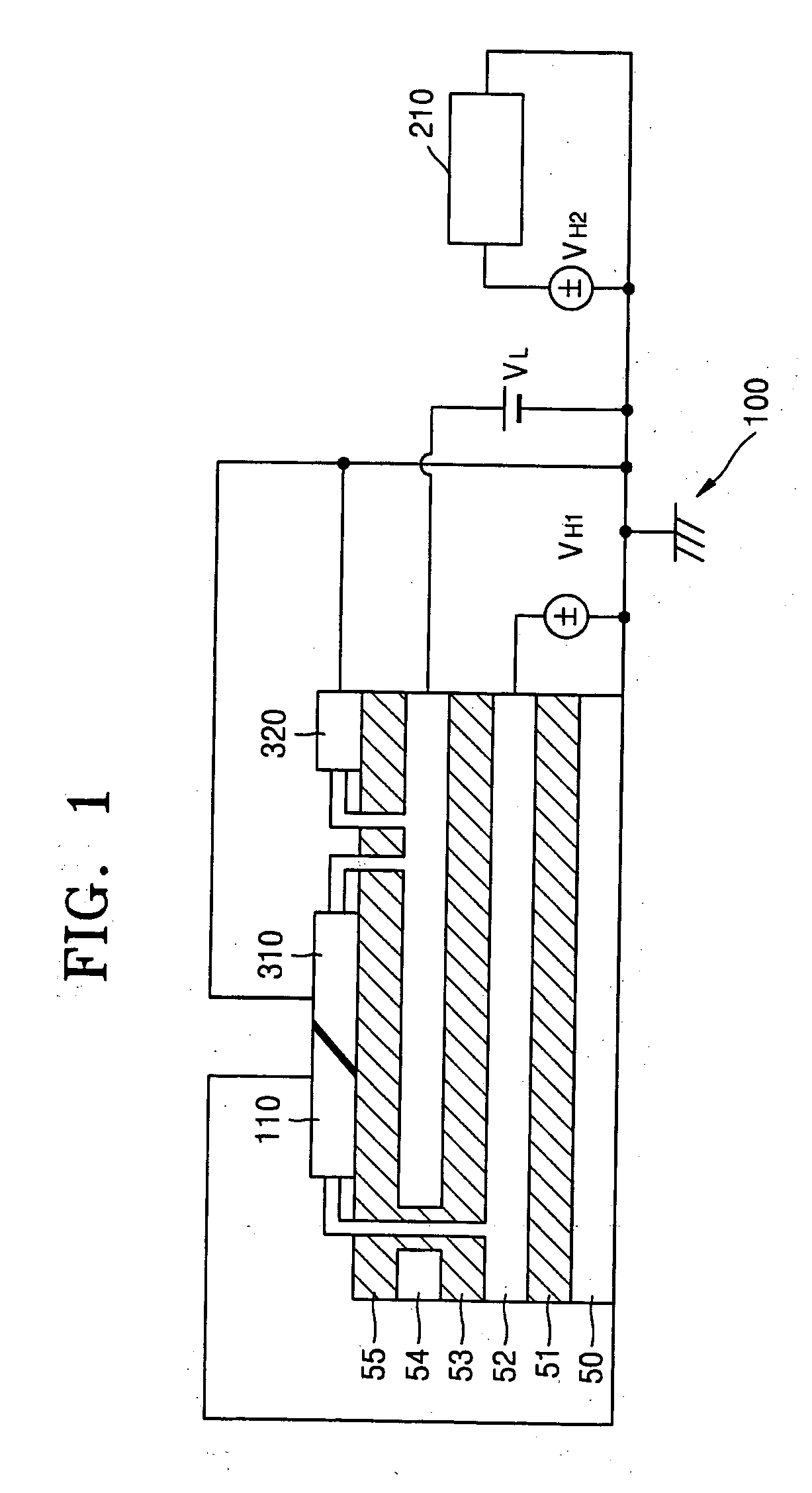
[0034]FIG. 1 is a schematic diagram illustrating low voltage elements (logic elements) and high voltage elements, which are commonly grounded in an EED. In FIG. 1, a left side includes a substrate on which high voltage elements 110 and low voltage elements 310 and 320 are mounted together, and a right side includes a high voltage element 210.

[0035] The low voltage logic element includes digital logic elements 310 and analog logic elements 320 and usually operates with ±5 V. As to the high voltage elements 210, a high voltage VH2 of ±50-100 V is supplied to a gate electrode line or data electrode line of the EED panel. A high voltage of about 4000 V is supplied to an anode. As to the digital logic elements 310, the driver is supplied with a high voltage VH1 in order to control a high voltage, which is supplied to the data electrode lines and scan electrode lines of the panel.

[0036] Therefore, the logic circuits,.such as the driver for controlling the high voltage VH1, are low volta...


PUM


Abstract

An EED capable of reducing noise influence between a high voltage element and a low voltage logic element in an EED panel includes: a high voltage ground for a high voltage element, a low voltage ground for a low voltage element, and a ferrite bead, connected between the high voltage ground and the low voltage ground, to block RF noise from the high voltage ground.

Description

CLAIM OF PRIORITY [0001] This application makes reference to, incorporates the same herein, and claims all benefits accruing under 35 U.S.C. §119 from an application for ELECTRON EMISSION DISPLAY WITH SEPARATED GROUNDS earlier filed in the Korean Intellectual Property Office on Apr. 29, 2004 and there duly assigned Serial No. 10-2004-0030007. BACKGROUND OF THE INVENTION [0002] 1. Field of the Invention [0003] The present invention relates to an Electron Emission Display (EED), and more particularly, to an EED which can reduce noise influence transferred through a ground between a high voltage element and a low voltage element. [0004] 2. Description of the Related Art [0005] An Electron Emission Display (EED) includes an EED panel and a driver. When the driver supplies a positive voltage to an anode of the EED panel, if a positive voltage is supplied to a gate electrode and a negative voltage is supplied to a cathode electrode, electrons are emitted from the cathode. The emitted elec...

Claims


Application Information

Patent Timeline
Patent Type & Authority Applications(United States)
IPC IPC(8): G09G3/22G09G3/20G09G3/30G09G5/00
CPCG09G2330/06G09G3/22A47G19/2227A47G2019/2244A47G2200/143
Inventor JEON, DONG-HYUP
Owner SAMSUNG SDI CO LTD
Why Eureka
Try Eureka