Voltage generator

a voltage generator and voltage technology, applied in the direction of pulse technique, process and machine control, instruments, etc., can solve the problems of conventional substrate bias voltage generators such as reducing the data holding time of drams

Inactive Publication Date: 2005-11-17
LAPIS SEMICON CO LTD
View PDF12 Cites 0 Cited by
  • Summary
  • Abstract
  • Description
  • Claims
  • Application Information

AI Technical Summary

Benefits of technology

[0009] However, since the DRAM is a type of memories which are driven at a high voltage, in cases where the first power supply voltage Vcc is set at high value, the substrate bias voltage Vbb has largely lowered conventionally in response to the level of the first power supply voltage. Vcc. If the substrate bias voltage Vbb lowers, which should be ideally always constant, even if the first power supply voltage Vcc rises, the difference in potential between the N+ type impurity region 121 and the P-type well 112 is made larger, so that the data holding time is cut down.

Problems solved by technology

That is, data leakage phenomenon occurs significantly, resulting in the reduction of data holding time of the DRAM.
The conventional substrate bias voltage generator has such a problem.

Method used


Image

  • Voltage generator
  • Voltage generator
  • Voltage generator

Examples


second embodiment

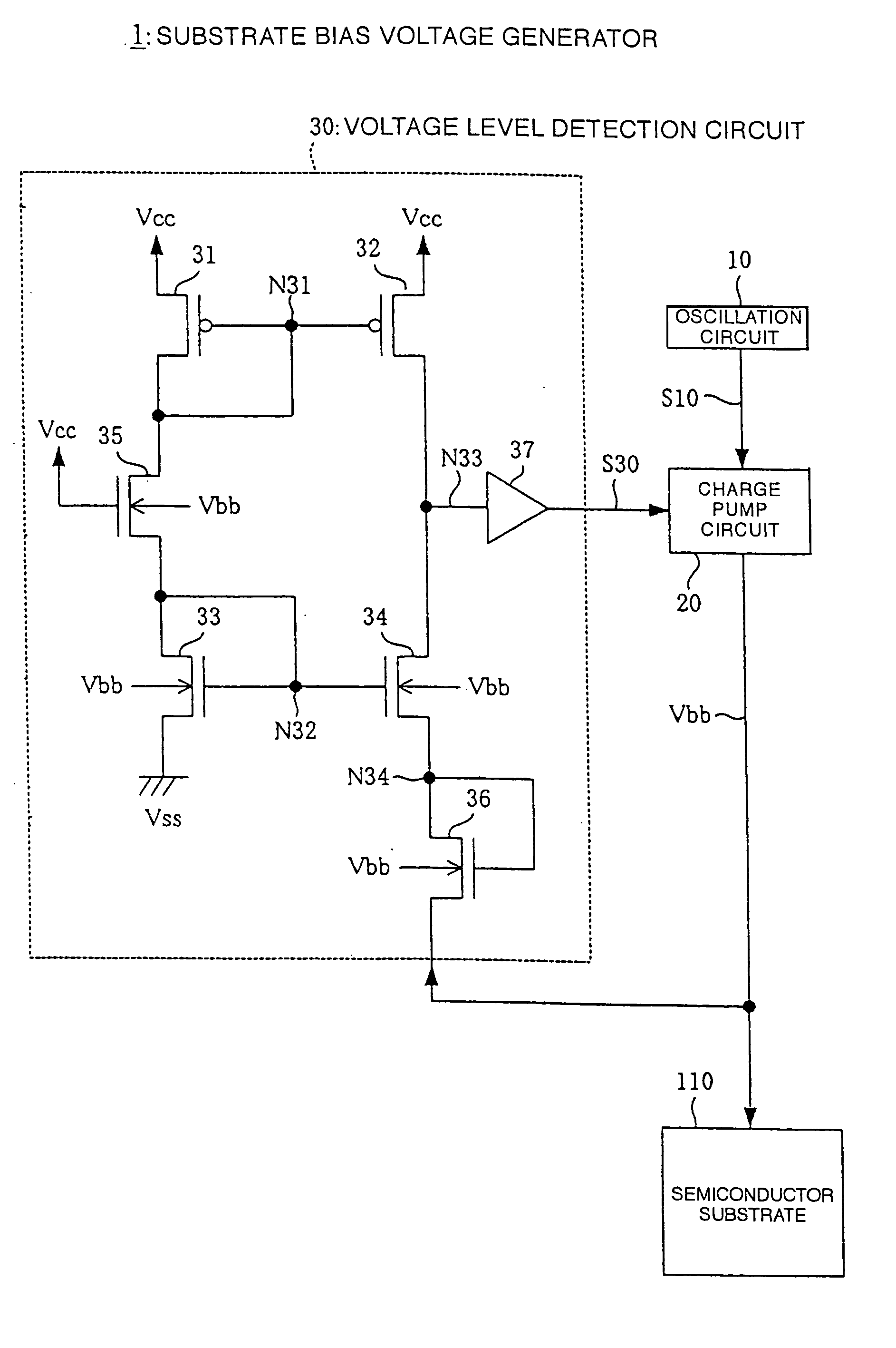
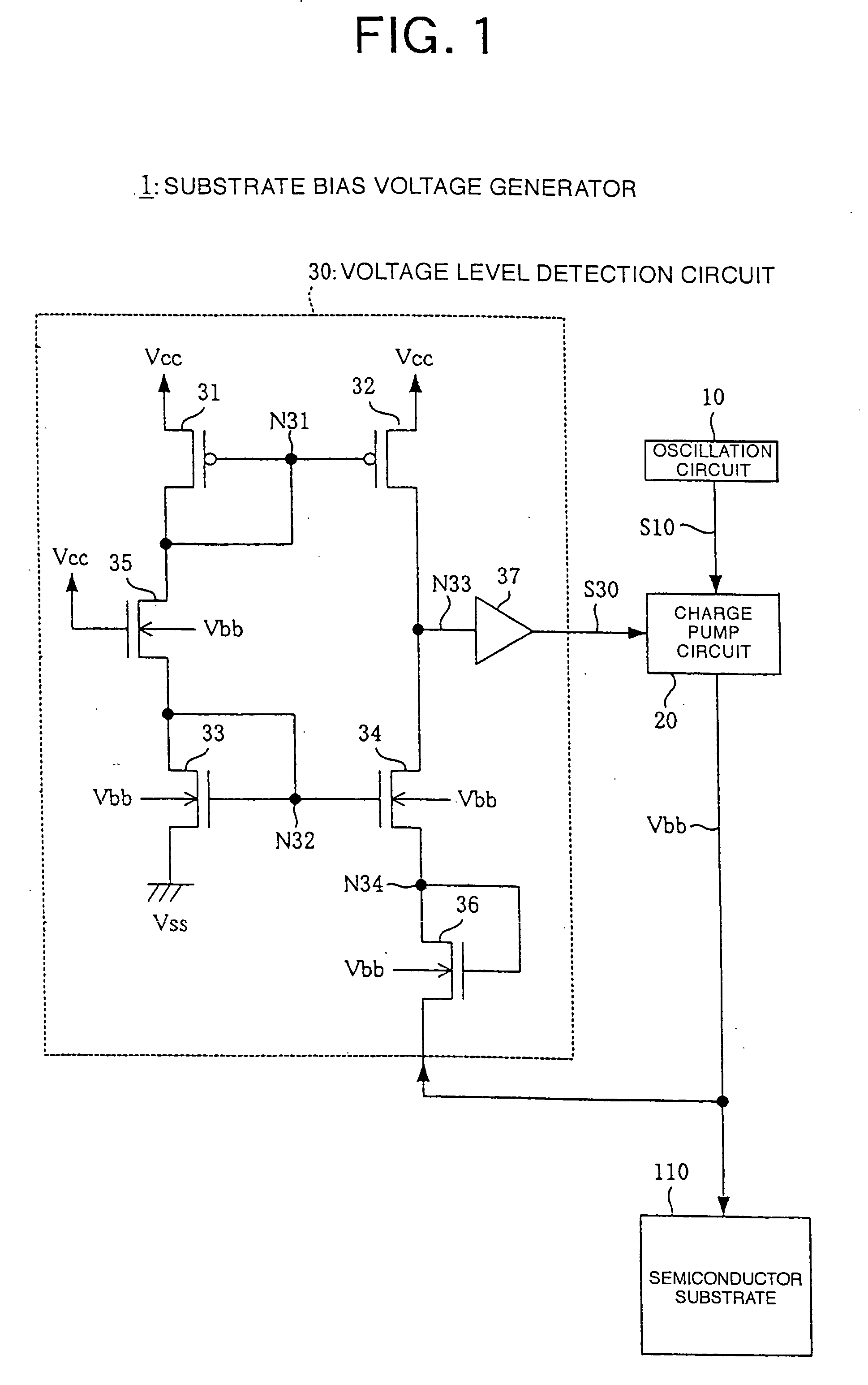
[0069] The configuration of a substrate bias voltage generator 2 according to the second embodiment of the invention is shown in FIG. 4. Comparing the substrate bias voltage generator 2 with the substrate bias voltage generator 1 of the first embodiment of the invention, the voltage level detection circuit 30 of the first embodiment is configured to be replaced with a voltage level detection circuit group 50. That is, the substrate bias voltage generator 2 comprises an oscillation circuit 10, a charge pump circuit 20, and the voltage level detection circuit group 50 and outputs a substrate bias voltage Vbb to be applied to a semiconductor substrate 110.

[0070] The voltage level detection circuit group 50 detects a level of the substrate bias voltage Vbb and outputs a voltage level detection signal S50 of H level or L level. The voltage level detection signal S50 is inputted to the charge pump circuit 20 as a signal for controlling the pumping operation of the charge pump circuit 20....


PUM


Abstract

When the substrate bias voltage Vbb lowers by the pumping operation of the charge pump circuit, a drain-to-source resistance of the N-transistor becomes high. When a first power supply voltage Vcc is set at high value, a drain-to-source current of the N-transistor increases (I+ΔI1), however the drain-to-source current decreases (I+ΔI1−ΔI2) by the increase of the drain-to-source current owing to the substrate bias effect so that the increase of the potential of the node N34 caused by the increase of the first power supply voltage VCC is restrained. As a result, a reference level of the substrate bias voltage Vbb does not largely lower than the reference level of the substrate bias voltage. Vbb when the first power supply voltage VCC is in a standard level.

Description

FIELD OF THE INVENTION [0001] The invention relates to a voltage generator, particularly to a voltage generator capable of keeping a potential of a semiconductor device at a given level. BACKGROUND OF THE INVENTION [0002] Each memory for constituting a DRAM (Dynamic Random Access Memory) is generally provided with an N-channel transistor (N-transistor) 100 and a capacitor 101. [0003] A drain of the N-transistor 100 is connected to a bit line BL, a gate thereof is connected to a word line WL and a source thereof is connected to a node N100. Further, a substrate bias voltage Vbb (e.g. −1.0V) which is outputted from a charge pump circuit (not shown) is applied to a back gate of the N-transistor 100. [0004] The capacitor 101 is formed, e.g. as a parallel flat plate type. One terminal of the capacitor 101 is connected to the node N100 while the other terminal thereof is connected to a node N101. A voltage which is half as much as a first power supply voltage Vcc is applied to the node N1...

Claims


Application Information

Patent Timeline
Patent Type & Authority Applications(United States)
IPC IPC(8): H01L27/04G05F3/20G05F3/24H01L21/822H03K19/00
CPCG05F3/205
Inventor YAMADA, HITOSHI
Owner LAPIS SEMICON CO LTD
Why Eureka
Try Eureka