Methods for transferring a useful layer of silicon carbide to a receiving substrate

a technology of silicon carbide and receiving substrate, which is applied in the direction of basic electric elements, electrical apparatus, semiconductor devices, etc., can solve the problems of incompatibility of the method with the transfer of a thin film of silicon carbide of good crystalline quality, the irregular surface of the source substrate, and the inability to polish the surface irregularities. to achieve the effect of facilitating the recycling of the remainder portion

Inactive Publication Date: 2005-12-01
SOITEC SA
View PDF13 Cites 187 Cited by
  • Summary
  • Abstract
  • Description
  • Claims
  • Application Information

AI Technical Summary

Benefits of technology

[0012] This technique includes implanting at least H+ ions through a front face of a source substrate of silicon carbide with an implantation energy E greater than or equal to 95 keV and an implantation dose D chosen to form an optimal weakened zone near a mean implantation depth, the optimal weakened zone defining the useful layer and a remainder portion of the source substrate. The method also includes bonding the front face of the source substrate to a contact face of the receiving substrate, and detaching the useful layer from the remainder portion of the source substrate along the weakened zone while minimizing or avoiding forming an excess zone of silicon carbide material at the periphery of the useful layer that was not transferred to the receiving substrate during detachment. Such a method facilitates recycling the remainder portion of the source substrate.

Problems solved by technology

However, after each layer transfer step, the upper surface of the source substrate has a certain number of surface irregularities.
In the specific case where the source substrate 1 is made of silicon carbide, an extremely hard material, such polishing steps are extremely long and costly.
This method is therefore incompatible with transferring a thin film of silicon carbide of good crystalline quality, since it is not possible to utilize a thin film from such a substrate for forming devices used in microelectronics or opto-electronics.

Method used


Image

  • Methods for transferring a useful layer of silicon carbide to a receiving substrate
  • Methods for transferring a useful layer of silicon carbide to a receiving substrate
  • Methods for transferring a useful layer of silicon carbide to a receiving substrate

Examples


Embodiment Construction

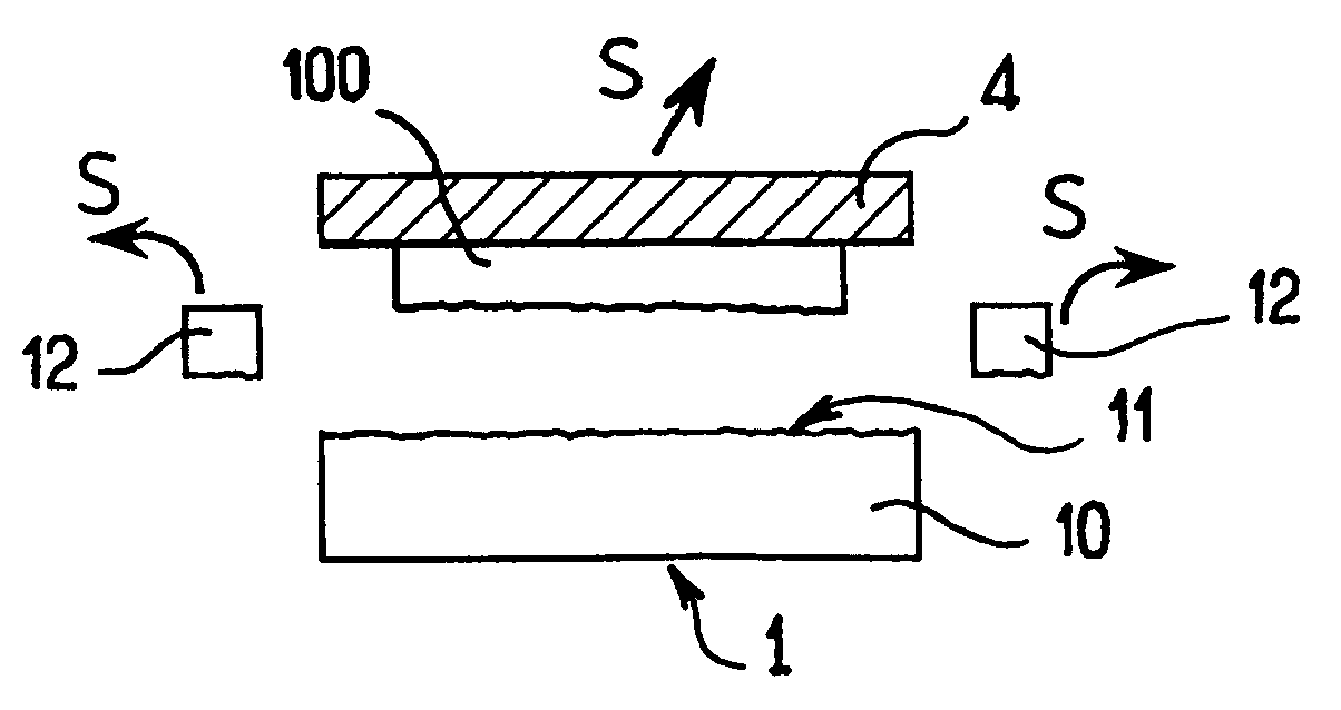
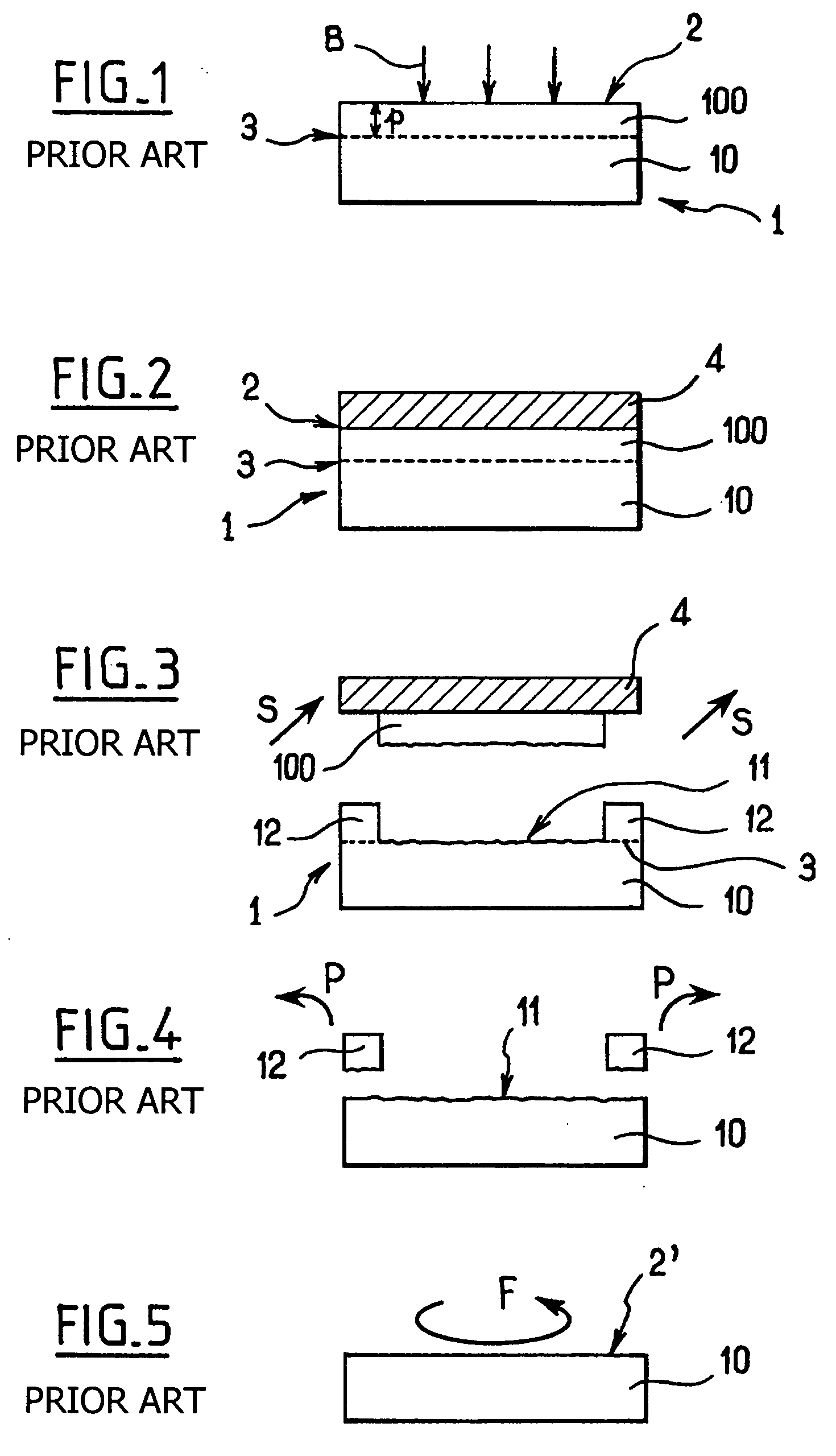
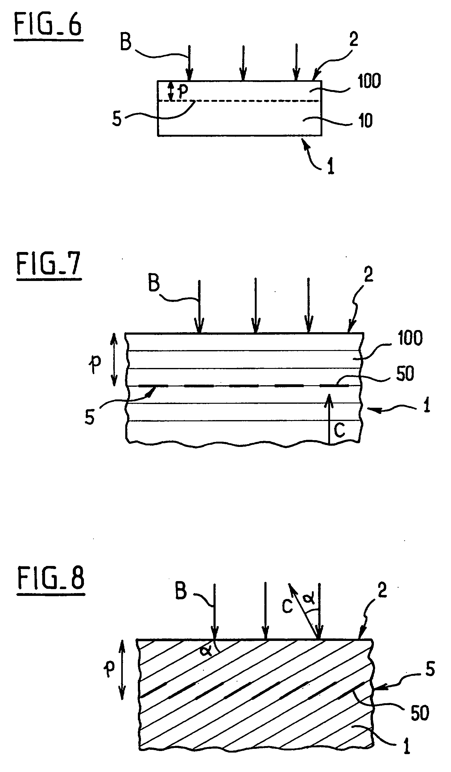
[0023] The methods according to the invention will now be described with reference to FIGS. 6-18. FIGS. 6-18 are similar to FIGS. 1-5, and identical elements have the same reference numerals.

[0024] Referring to FIG. 6, a goal of the invention is to optimize the implantation conditions B of atomic species within a source substrate 1 of monocrystalline silicon carbide. In particular, it is desired to create an “optimal weakened zone”5 in the neighborhood of the mean depth p of ion implantation, so that it is possible to remove or exfoliate, after the useful layer 100 is detached and after an appropriate thermal budget is applied, 100% or substantially about 100% of the blistered excess zone 12 which remained integral to the remainder 10 of the source substrate in the prior art (see FIG. 3). “Optimally weakening” means introducing atomic species into the crystal in a precise and controlled manner in order to optimally activate the weakened mechanisms used. The implantation of atomic s...


PUM

PropertyMeasurementUnit
energyaaaaaaaaaa
temperatureaaaaaaaaaa

Abstract

Methods for transferring a useful layer of silicon carbide to a receiving substrate are described. In an embodiment, the invention relates to a method for recycling of a silicon carbide source substrate by removal of the excess zone followed by a finishing step to prepare the source substrate for recycling and reuse. Preferably, the excess zone is removed by a thermal budget where the temperature and time of such treatment causes exfoliation of the excess zone. The finishing step is performed in a manner to provide the desired surface roughness for the substrate so that it can be recycled for re-use. The technique includes implanting at least H+ ions through a front face of a source substrate of silicon carbide with an implantation energy E greater than or equal to 95 keV and an implantation dose D chosen to form an optimal weakened zone near a mean implantation depth, the optimal weakened zone defining the useful layer and a remainder portion of the source substrate. The method also includes bonding the front face of the source substrate to a contact face of the receiving substrate, and detaching the useful layer from the remainder portion of the source substrate along the weakened zone while minimizing or avoiding forming an excess zone of silicon carbide material at the periphery of the useful layer that was not transferred to the receiving substrate during detachment.

Description

CROSS-REFERENCE TO RELATED APPLICATIONS [0001] This application is a division of application Ser. No. 10 / 893,192 filed Jul. 15, 2004, which is a continuation of International application no. PCT / EP03 / 00692 filed Jan. 21, 2003, the entire content of each of which is expressly incorporated herein by reference thereto.BACKGROUND ART [0002] The present invention relates to an optimized method for transferring an useful layer of monocrystalline silicon carbide (SiC) derived from a source substrate of the same material to a receiving or stiffening substrate. The method permits recycling of the substrate after the transfer of the thin useful layer. [0003] The method known under the trademark “SMART-CUT®” enables a thin layer to be transferred from a source substrate to a receiving substrate such as, for example, an oxidized silicon or polycrystalline silicon carbide substrate. This method also enables the source substrate from which the thin layer has been taken to be reused. However, afte...

Claims


Application Information

Patent Timeline
Patent Type & Authority Applications(United States)
IPC IPC(8): H01L21/02H01L21/18H01L21/20H01L21/266H01L21/76H01L21/265H01L21/762H01L27/12
CPCH01L21/02032H01L21/187H01L21/2007H01L21/76254H01L21/266H01L21/7602H01L21/26586H01L21/20
Inventor GHYSELEN, BRUNOLETERTRE, FABRICE
Owner SOITEC SA
Why Eureka
Try Eureka