

Input buffer structure with single gate oxide
a buffer and input technology, applied in the field of integrated circuits, can solve the problems of inability to provide sufficient driving current for inverters, the design of such buffers is becoming increasingly difficult, and the communication between these different devices is becoming more complex
- Summary
- Abstract
- Description
- Claims
- Application Information
AI Technical Summary
Benefits of technology
Problems solved by technology
Method used
Image

Examples
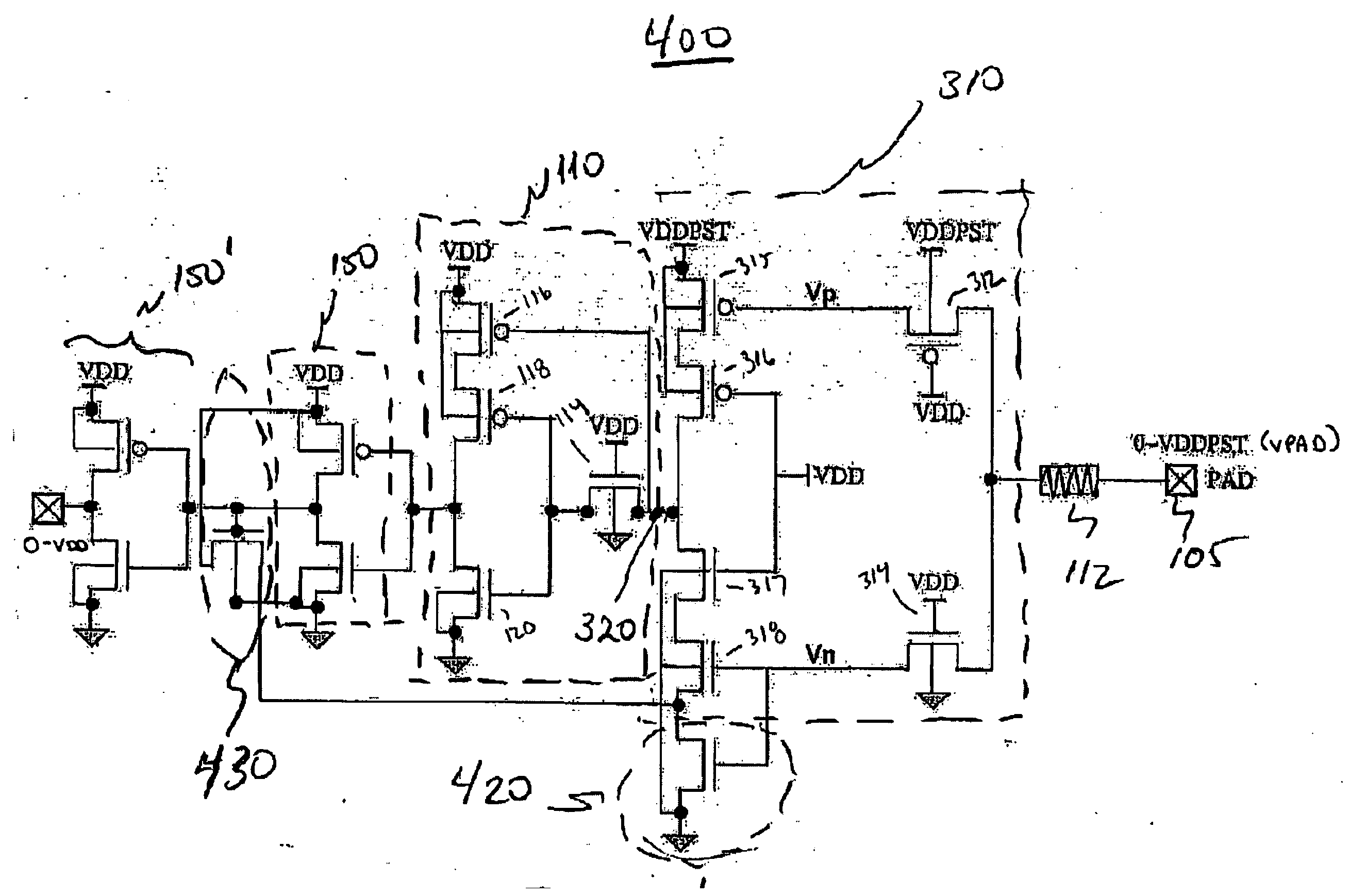
exemplary embodiment 400
[0030]FIG. 4 illustrates a second exemplary embodiment 400 of a single gate oxide input buffer. In this embodiment, which is similar to that shown in FIG. 3, transistors 420 and 430 are incorporated to act as a Schmitt trigger. A Schmitt trigger is an electronic circuit that produces an output when the input exceeds a predetermined turn-on or threshold level. The output is maintained until the input falls below the threshold level.
[0031] At the rising edge of the input level at pad 105, the output of the inverter stage 150 is high. The NMOS 430 is turned on and a feedback voltage of VDD-Vthn is passed to the drain of NMOS 420 and the low to high threshold point is thus increased. The source voltage at NMOS 318 is elevated through the feedback path. Therefore, the voltage Vn must be higher than Vthn to turn on NMOS 318, thereby increasing noise immunity. Assume, as shown in FIG. 6, that the trigger point for the embodiment 300 described above without the Schmitt trigger is 1.25V. The...
exemplary embodiment 500
[0032]FIG. 5 illustrates a third exemplary embodiment 500 of a single gate oxide input buffer. In this embodiment circuit 510 is coupled between the threshold adjusting circuit 310 and level down stage 110. Circuit 510 comprises circuits 520 and 530 and operates as a Schmitt trigger in a manner similar to that shown in FIG. 4. Each circuit 520 and 520 includes a pair of cross-coupled transistors coupled between the output node 320 and the inverter of threshold adjustment stage 310. More specifically, during the rising edge of the input signal at pad 105, the output voltage of circuit 310 is VDDPST and a feedback voltage of VDD-Vthn is passed to the source of NMOS 318 via circuit 530. The output level of circuit 310 does not become zero until the NMOS 318 is fully turned on. As described in connection with FIG. 4, the low to high threshold point is elevated above half VDDPST due to the feedback voltage through 530.
[0033] During the falling edge of the signal at 105, the output voltag...
PUM
 Abstract
Description
Claims
Application Information