Nonvolatile semiconductor memory and fabrication method for the same

a fabrication method and semiconductor technology, applied in semiconductors, electrical devices, transistors, etc., can solve the problems of structure impairing the cutoff characteristics of transistors

Inactive Publication Date: 2007-02-22
KK TOSHIBA
View PDF18 Cites 19 Cited by
  • Summary
  • Abstract
  • Description
  • Claims
  • Application Information

AI Technical Summary

Benefits of technology

[0012] An aspect of the present invention inheres in a nonvolatile semiconductor memory comprising a cell array region that includes aligned memory cell transistors, each including a control gate electrode. The control gate electrode includes a first metal silicide film, an inter-gate insulating film under the control gate electrode, a floating gate electrode under the inter-gate insulating film, and a tunnel insulating film under the floating gate electrode. A high-voltage circuit region is arranged in a periphery of the cell array region and includes a high voltage transistor, which includes a gate electrode and a first gate insulating film, thicker than the tunnel insulating film, below the gate electrode. A low-voltage circuit region is arranged in a different position than the high-voltage circuit region arranged in the periphery of the cell array region and includes a low-voltage transistor, which includes a gate electrode and a second gate insulating film, thinner than the first gate insulating film, below the gate electrode. A tunnel insulating film is directly provided on source regions and drain regions of the respective memory cell transistors, and a liner insulating film is directly provided on source regions and drain regions of the high-voltage transistors and the low-voltage transistors.
[0013] Another aspect of the present invention inheres in a fabrication method for a nonvolatile semiconductor memory, which includes a cell array region, a high-voltage circuit region, and a low-voltage circuit region. The fabrication method comprises depositing a tunnel insulating film on a semiconductor substrate, a floating gate electrode layer on the tunnel insulating film, and a stopper film on the floating gate e...

Problems solved by technology

This structure impairs cutoff characteristic...

Method used


Image

  • Nonvolatile semiconductor memory and fabrication method for the same
  • Nonvolatile semiconductor memory and fabrication method for the same
  • Nonvolatile semiconductor memory and fabrication method for the same

Examples


first embodiment

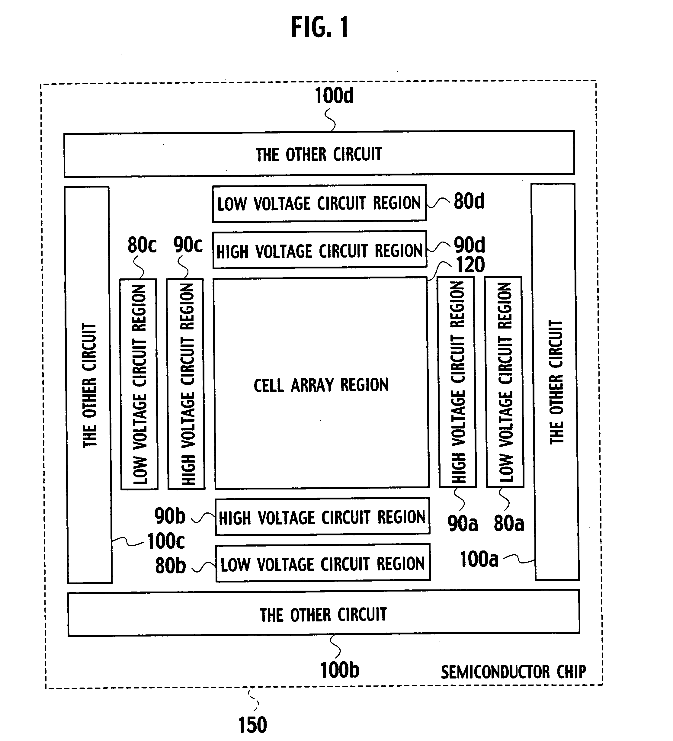
[0215] As shown in FIG. 1, a schematic block structure of a nonvolatile semiconductor memory, according to the first embodiment of the present invention, includes a cell array region 120 deployed on a semiconductor chip 150, high-voltage circuit regions 90a, 90b, 90c, and 90d arranged adjacent to each other on the four sides of the cell array region 120, low-voltage circuit regions 80a, 80b, 80c, and 80d arranged adjacent to the high-voltage circuit regions 90a, 90b, 90c, and 90d, respectively, and other circuit regions 100a, 100b, 100c, and 100d arranged adjacent to the low-voltage circuit regions 80a, 80b, 80c, and 80d, respectively. The circuit regions 100a, 100b, 100c, and 100d are regions in which low-voltage circuits, high voltage circuits, and resistor regions are arranged. The high-voltage circuit regions 90a, 90b, 90c, and 90d apply relatively higher voltage pulses compared to power-supply voltages, such as a write-in voltage Vpgm and an erase voltage Verase, to the cell ar...

second embodiment

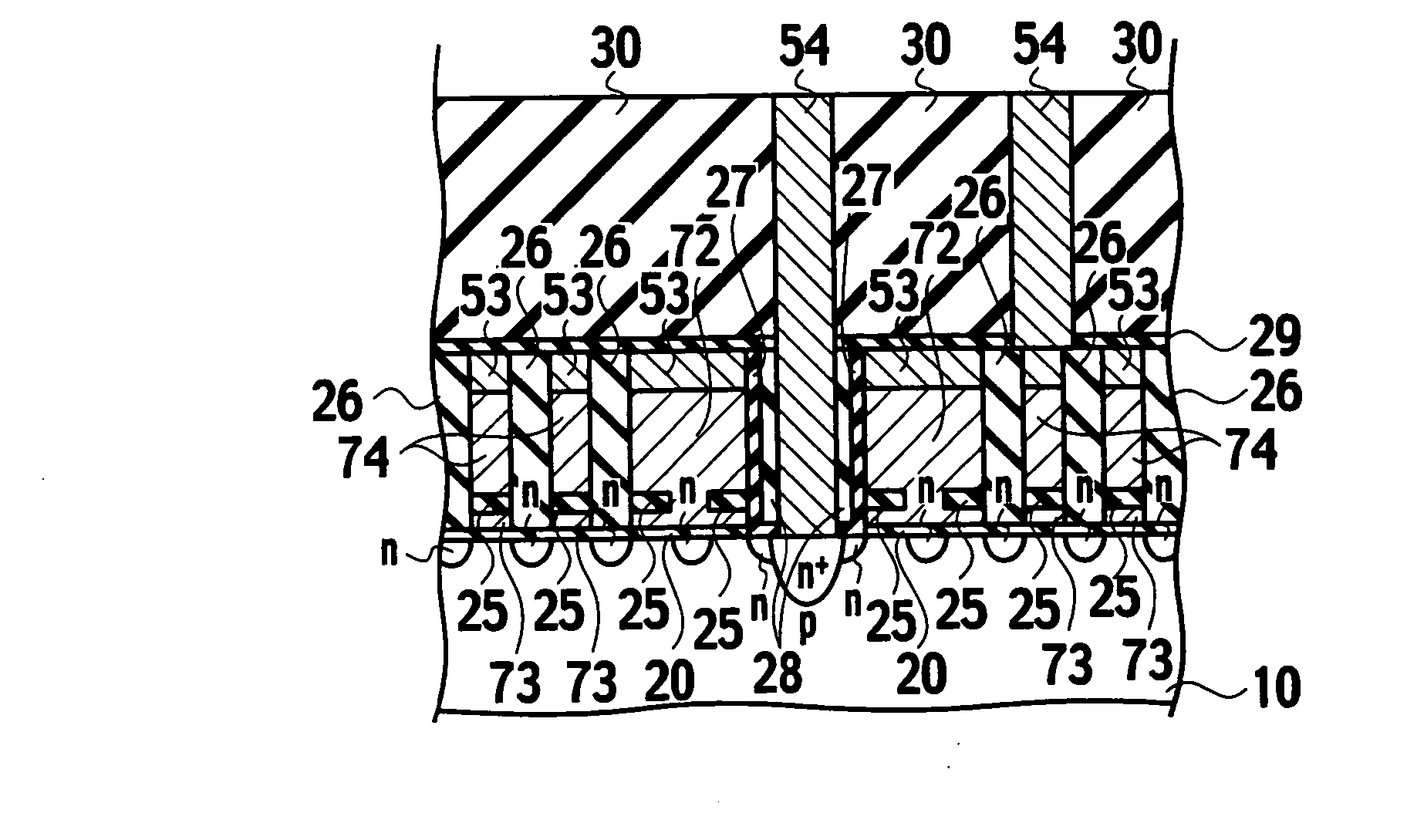
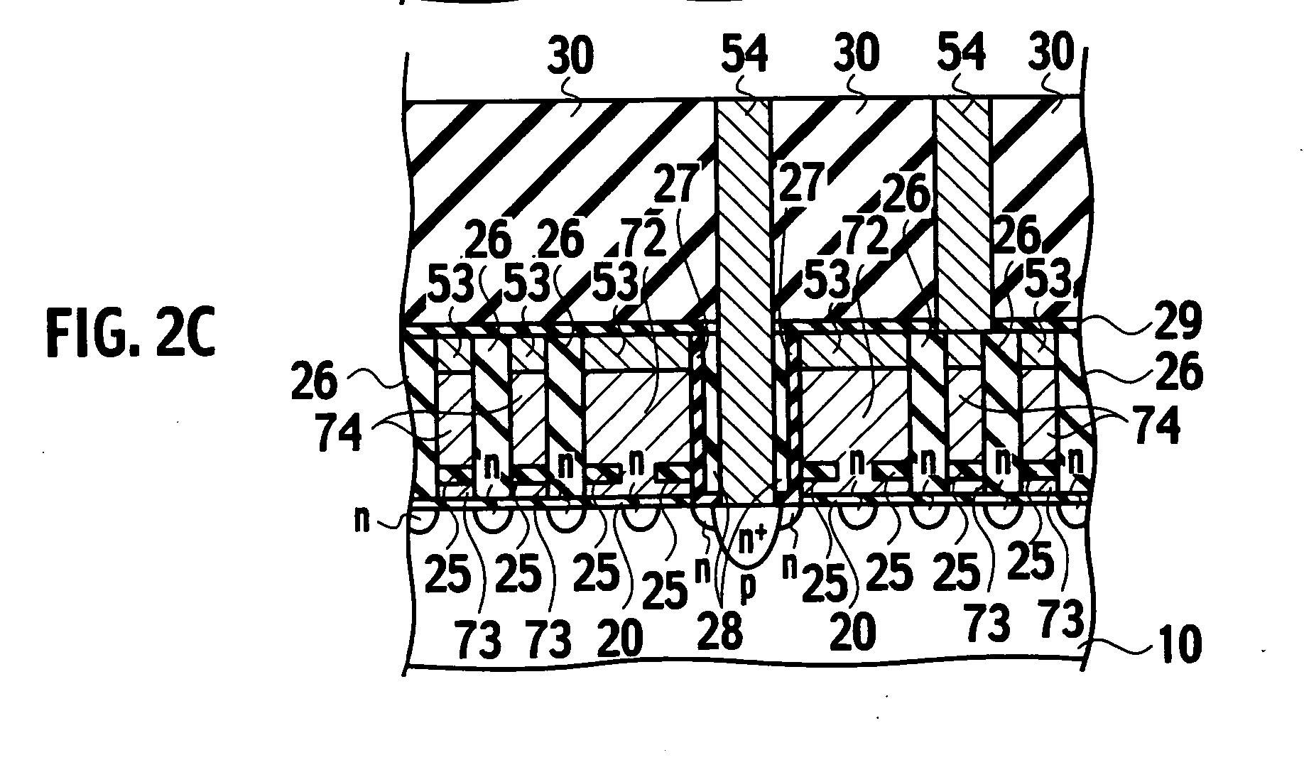
[0235] A nonvolatile semiconductor memory according to the second embodiment of the present invention, as shown in FIG. 23C, differs from the nonvolatile semiconductor memory according to the first embodiment, shown in FIG. 2C in that the gate sidewall insulating films 75, as made to be thinner, are remained at the gate sidewall region in addition to the liner insulating film 27. During contact formation of contacts 54, the first interlayer insulating film 28 on contact openings of contacts 54 may be completely removed or part thereof may be left at the gate sidewall region of contact openings of contacts 54, using the liner insulating film 27 as a stopper film. Contacts 54 are formed in a self-aligned manner in select transistors covered by the liner insulating films 27. The remainder of the structure is substantially the same as the nonvolatile semiconductor memory shown in FIGS. 2A through 2C, and thus repetitive description is omitted.

[0236] A nonvolatile semiconductor memory f...

third embodiment

[0244] A nonvolatile semiconductor memory according to the third embodiment of the present invention, as shown in FIG. 31B, differs from the nonvolatile semiconductor memory shown in FIG. 2B in that masking material 23 is deployed, instead of the metal silicide films 53, on the gate electrodes 71 of the transistors in the high-voltage circuit regions 90a, 90b, 90c, and 90d. The remainder of the description is substantially the same as the nonvolatile semiconductor memory shown in FIGS. 2A through 2C, and thus repetitive description is omitted.

[0245] A nonvolatile semiconductor memory fabricating process according to the third embodiment is described while referencing FIGS. 31 through 38. FIGS. 31A through 38A are schematic cross sections of a transistor in the low-voltage circuit regions 80a, 80b, 80c, and 80d. FIGS. 31B through 38B are schematic cross sections of a transistor in the high-voltage circuit regions 90a, 90b, 90c, and 90d. FIGS. 31C through 38C are cross sections cut a...


PUM


Abstract

The present invention provides a nonvolatile semiconductor memory that allows simultaneous implementation of high performance transistors in a low-voltage circuit region and transistors with high withstand voltages in a high-voltage circuit region. The nonvolatile semiconductor memory includes a cell array region that comprises aligned memory cell transistors, each including a control gate electrode, which includes a metal silicide film, an inter-gate insulating film below the control gate electrode, a floating gate electrode below the inter-gate insulating film, and a tunnel insulating film under the floating gate electrode; a high-voltage circuit region arranged in a periphery of the cell array region and including a high voltage transistor, which includes a first gate insulating film thicker than the tunnel insulating film; and a low-voltage circuit region that is arranged in a different position than the high-voltage circuit region arranged in the periphery of the cell array region and that includes a low-voltage transistor, which includes a gate electrode and a second gate insulating film thinner than the first gate insulating film below the gate electrode.

Description

CROSS REFERENCE TO RELATED APPLICATIONS AND INCORPORATION BY REFERENCE [0001] This application is based upon and claims the benefit of priority from prior Japanese Patent Application P2005-185616 filed on Jun. 24, 2005; the entire contents of which are incorporated by reference herein. BACKGROUND OF THE INVENTION [0002] 1. Field of the Invention [0003] The present invention relates to nonvolatile semiconductor memory and a fabrication method for the same. More specifically, it relates to a nonvolatile semiconductor memory used for a flash memory and a fabrication method for the same. [0004] 2. Description of the Related Art [0005] An electronically erasable programmable read-only memory (EEPROM), for example, is well-known as a conventional nonvolatile semiconductor memory. In an EEPROM, particularly in the case of a NAND type, memory cells are deployed at respective intersections where word lines extending in a row and bit lines extending in a column cross each other, constituting ...

Claims


Application Information

Patent Timeline
IPC IPC(8): H01L29/788
CPCH01L27/115H01L27/11526H01L27/11529H10B41/41H10B41/40H10B69/00H10B41/35H10B63/30
Inventor MATSUNAGA, YASUHIKO
Owner KK TOSHIBA
Why Eureka
Try Eureka