High performance FET with elevated source/drain region

a field effect transistor, high-performance technology, applied in the direction of transistors, semiconductor devices, electrical equipment, etc., can solve the problems of limiting current supplied, slow capacitive switching, rapid increase of static power consumption, etc., to improve the performance of field effect transistors, reduce device resistances, and reduce ultra-thin channel fet series resistance.

Inactive Publication Date: 2005-03-08
IBM CORP
View PDF13 Cites 107 Cited by
  • Summary
  • Abstract
  • Description
  • Claims
  • Application Information

AI Technical Summary

Benefits of technology

It is a purpose of the invention to improve field effect transistor (FET) performance;
It is another purpose of the invention to reduce ultra-thin channel FET series resistance.
The present invention relates to a field effect transistor (FET), integrated circuit (IC) chip including the FETs and a method of forming the FETs. The FETs include a thin channel with raised source / drain (RSD) regions at each end on an insulator layer, e.g., on an ultra-thin silicon on insulator (SOI) chip. Isolation trenches at each end of the FETs, i.e., at the end of the RSD regions, isolate and define FET islands. Insulating sidewalls at each RSD region sandwich the FET gate between the RSD regions. The gate dielectric may be a high K dielectric. Salicide on the RSD regions and, optionally, on the gates reduce device resistances.

Problems solved by technology

Device resistances limit current supplied by a particular device and slow capacitive switching.
Another design concern is that, as FET features have shrunk, what are collectively known as short channel effects have become pronounced, resulting in a rapid increase of static power consumption.
Unfortunately, especially as FET features have shrunk, thinner gate insulator (e.g., silicon oxide (SiO2) or a high-K dielectric) has resulted in increased gate leakages or gate induced leakages (i.e., gate to channel, gate to source or drain and gate induced drain leakage (GIDL)).
Unfortunately, however, forming source / drain regions that are made from the same ultra-thin silicon layer increases external resistance and in particular contact resistance.
Similar high resistance source / drain diffusion and contact problems have been encountered in bulk silicon CMOS with lightly doped drain (LDD) devices, where the source / drain regions are maintained very shallow for lower voltage operation.
Especially for these very short devices, unless the source / drain silicide is spaced away from the gate, the silicide can cause gate to channel or source / drain shorts, for example.
Also, silicide can interfere / interact with high-K gate dielectric formation and vice versa.
However, thickening the silicon layer to form RSD regions has also suffered from inadequate isolation and so, has suffered from an increase in source to drain shorts.

Method used


Image

  • High performance FET with elevated source/drain region
  • High performance FET with elevated source/drain region
  • High performance FET with elevated source/drain region

Examples


Embodiment Construction

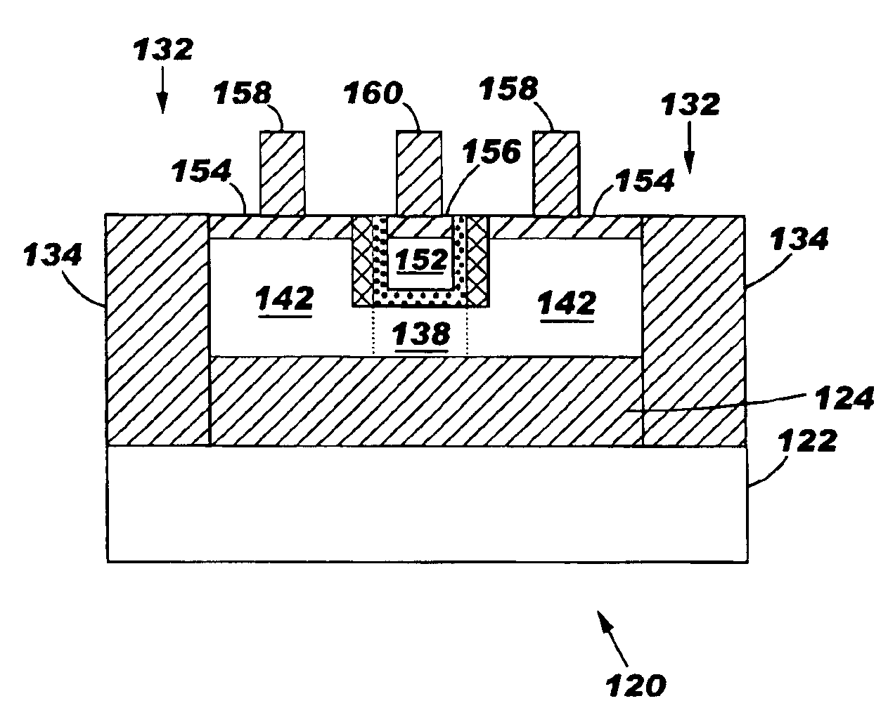
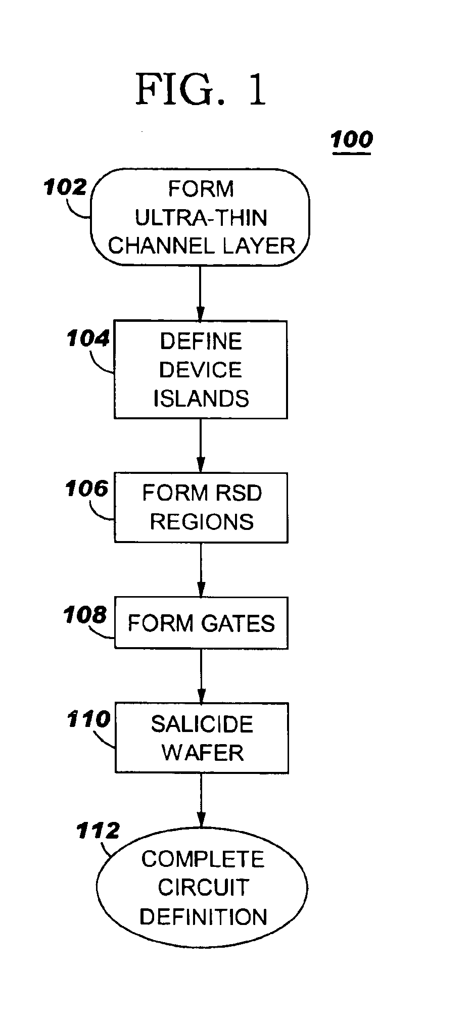
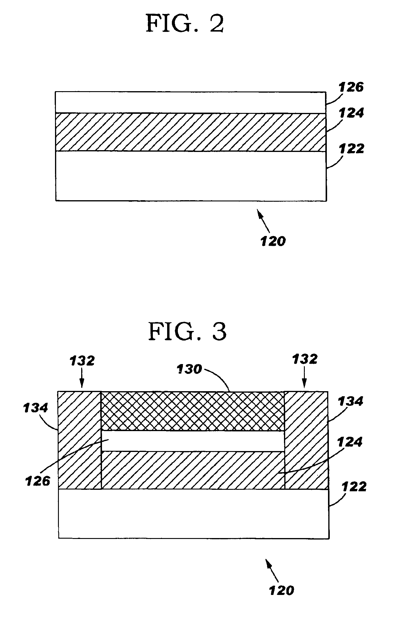
Turning now to the drawings and, more particularly, FIG. 1 shows a flow diagram example 100 for forming field effect transistors (FETs) with raised source / drain (RSD) regions according to a preferred embodiment of the present invention. First, in step 102 a layered semiconductor (e.g., silicon) on insulator (SOI) wafer is provided with an ultra-thin semiconductor surface layer. Next, in step 104 device islands are formed from the ultra-thin semiconductor surface layer, e.g., using shallow trench isolation (STI). Then, in step 106 source / drain regions are thickened on the islands. In step 108 damascene replacement gates are formed between and using the RSD regions as a stopping layer, which competes individual device structure at each device island. For a typical CMOS SOI chip, steps 104, 106 and 108 can each be performed for one type device followed by the second (e.g., P-type followed by N-type or vice versa) or each of steps 104, 106 and 108 may be performed for the one type, imme...


PUM


Abstract

The invention includes a field effect transistor (FET) on an insulator layer, and integrated circuit (IC) on SOI chip including the FETs and a method of forming the IC. The FETs include a thin channel with raised source/drain (RSD) regions at each end on an insulator layer, e.g., on an ultra-thin silicon on insulator (SOI) chip. Isolation trenches at each end of the FETs, i.e., at the end of the RSD regions, isolate and define FET islands. Insulating sidewalls at each RSD region sandwich the FET gate between the RSD regions. The gate dielectric may be a high K dielectric. Salicide on the RSD regions and, optionally, on the gates reduce device resistances.

Description

BACKGROUND OF THE INVENTION1. Field of the InventionThe present invention is related to semiconductor devices and more particularly to high performance field effect transistors (FETs) and methods of manufacturing high performance FETs.2. Background DescriptionTypical semiconductor integrated circuit (IC) design goals include high performance (circuit switching frequency) and density (transistors per unit area) at minimum circuit power. Semiconductor technology and chip manufacturing advances have continually reduced circuit feature dimensions and, correspondingly, supply voltage to pack more function in the same area. To minimize power, many ICs are made in the well-known complementary insulated gate field effect transistor (FET) technology known as CMOS.A typical CMOS circuit drives a purely or nearly pure capacitive load and includes paired complementary devices, i.e., an n-type FET (NFET) paired with a corresponding p-type FET (PFET), usually gated by the same signal. A CMOS inve...

Claims


Application Information

Patent Timeline
Patent Type & Authority Patents(United States)
IPC IPC(8): H01L21/02H01L29/66H01L21/336H01L29/76H01L29/45H01L29/786
CPCH01L29/458H01L29/66545H01L29/66553H01L29/78684H01L29/66772H01L29/7842H01L29/78618H01L29/66628H01L29/665
Inventor DIVAKARUNI, RAMAHSU, LOUIS C.JOSHI, RAJIV V.RADENS, CARL J.
Owner IBM CORP
Why Eureka
Try Eureka