Buried silicide structure and method for making

a silicide structure and silicide technology, applied in semiconductor devices, digital storage, instruments, etc., can solve the problem of reducing the loading effect of silicon material in semiconductor lines, and achieve the effect of being ready to manufactur

Active Publication Date: 2010-12-02
MACRONIX INT CO LTD
View PDF33 Cites 105 Cited by
  • Summary
  • Abstract
  • Description
  • Claims
  • Application Information

AI Technical Summary

Benefits of technology

[0017]A memory device as described herein can be readily manufactured using the processes described herein and includes a first array of memory cells underlying a second array of memory cells, the first and second arrays of memory cells separated from one another by an insulator layer. The first array of memory cells comprises a plurality of word lines comprising doped silicon material, with silicide conductors below top surfaces of the

Problems solved by technology

The higher electrical conductivity of the silicide lines thus reduces

Method used


Image

  • Buried silicide structure and method for making
  • Buried silicide structure and method for making
  • Buried silicide structure and method for making

Examples


Embodiment Construction

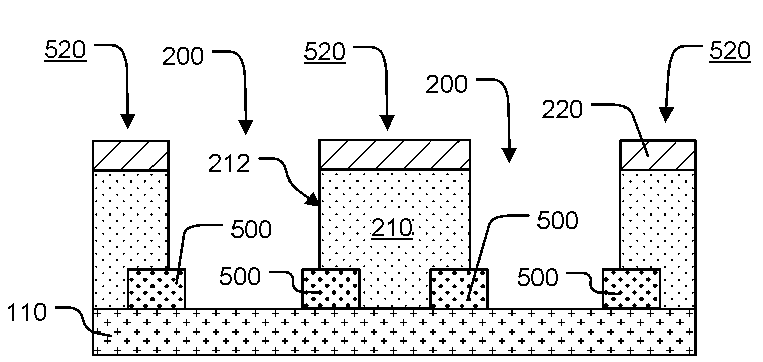
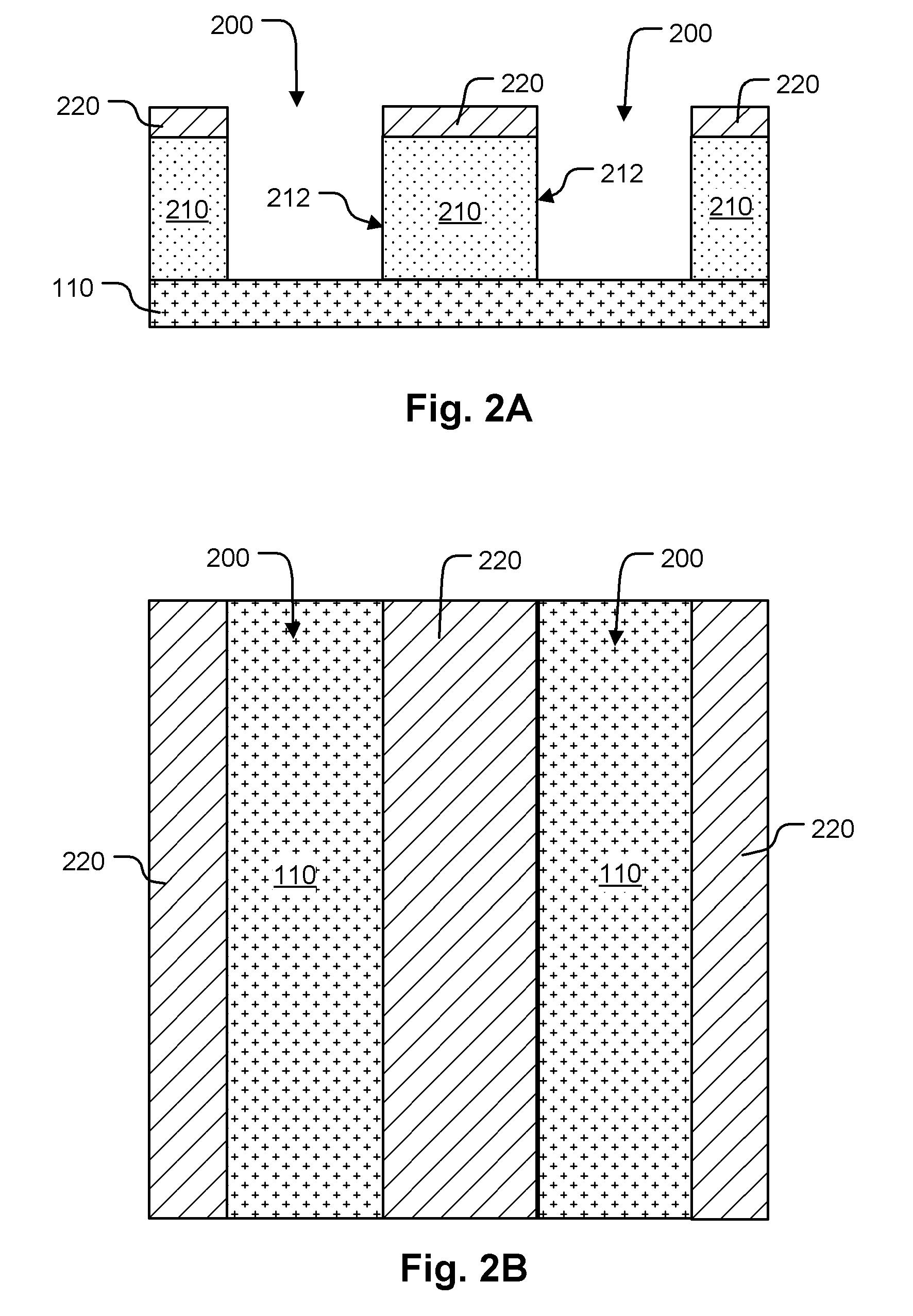
[0032]FIGS. 1-5 illustrate an embodiment of steps in a fabrication sequence for manufacturing buried silicide lines to reduce the loading effect of doped silicon material.

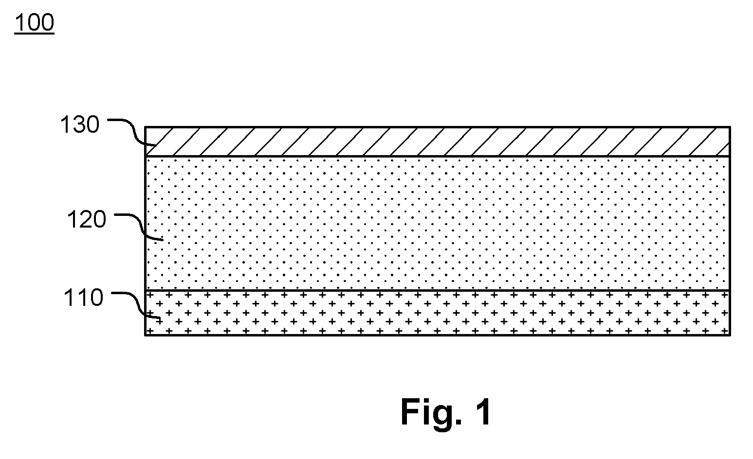
[0033]FIG. 1 illustrates a cross-sectional view of a step of forming a semiconductor body 100 by forming a layer of doped silicon 120 on an insulator layer 110, and forming a protection layer 130 on the layer of silicon 120. The layer of silicon 120 may be formed on the insulator layer 110, for example, using silicon-on-insulator techniques or the like. In the illustrated embodiment the insulator layer 110 comprises silicon dioxide.

[0034]The protection layer 130 can serve as an etch stop layer for the subsequent process steps described below. In the illustrated embodiment the protection layer 130 comprises silicon nitride. Alternatively, other materials may be used.

[0035]Next, a plurality of trenches 200 are formed through the protection layer 130 and the layer of silicon 120 to expose portions of the insulator lay...


PUM


Abstract

Methods for manufacturing buried silicide lines are described herein, along with high density stacked memory structures. A method for manufacturing an integrated circuit as described herein includes forming a semiconductor body comprising silicon. A plurality of trenches are formed in the semiconductor body to define semiconductor lines comprising silicon between adjacent trenches, the semiconductor lines having sidewalls. A silicide precursor is deposited within the trenches to contact the sidewalls of the semiconductor lines, and a portion of the silicide precursor is removed to expose upper portions of the sidewalls and leave remaining strips of silicide precursor along the sidewalls. Silicide conductors are then formed by inducing reaction of the strips of silicide with the silicon of the semiconductor lines.

Description

BACKGROUND OF THE INVENTION[0001]1. Field of the Invention[0002]The present invention relates to high density integrated circuit devices including buried silicide conductors, and to methods for manufacturing such devices.[0003]2. Description of Related Art[0004]One common technology for interconnecting components on integrated circuits is the use of buried diffusion lines, which consist of lines of implanted dopants in relatively high concentration, so that they act as electrical conductors in the substrate.[0005]A problem that arises with the use of buried diffusion lines is the loading effect due to their relatively high resistance. In operation, the relatively large resistance of the implanted dopants compared to that of metal results in increased power consumption and a reduction in the operation speed of the device. As a result, various techniques have been used to reduce the loading effect of the buried diffusion lines.[0006]One approach is to reduce the resistance of the line...

Claims


Application Information

Patent Timeline
IPC IPC(8): H01L45/00H01L21/768
CPCH01L21/743H01L45/1683H01L27/0688H01L27/101H01L27/2409H01L27/2472H01L27/2481H01L45/04H01L45/06H01L45/085H01L45/1233H01L45/142H01L45/144H01L45/146H01L45/147H01L45/1625H01L45/1675H01L21/8221H10B63/20H10B63/82H10B63/84H10N70/20H10N70/245H10N70/231H10N70/8822H10N70/8836H10N70/026H10N70/826H10N70/8828H10N70/8833H10N70/063H10N70/066
Inventor CHEN, SHIH-HUNGHONG, TIAN-JUE
Owner MACRONIX INT CO LTD
Why Eureka
Try Eureka