One step salicide process without bridging

a salicide and titanium technology, applied in the field of semiconductor devices, can solve the problems of reducing the performance of mos and other types of integrated circuits, converting titanium to titanium silicide in undesirable regions, and polysilicon electrodes that form the gates of mos devices

Inactive Publication Date: 2000-01-11
UNITED MICROELECTRONICS CORP
View PDF14 Cites 89 Cited by
  • Summary
  • Abstract
  • Description
  • Claims
  • Application Information

AI Technical Summary

Problems solved by technology

As line widths and geometries for semiconductor devices are made smaller, the polysilicon electrodes that form the gates of MOS devices and wiring lines within semiconductor devices become undesirably resistive.
While it has become important to provide reduced conductivity gate electrodes in high density integrated circuit devices, there have been significant difficulties in implementing this technology in a reliable manner that predictably achieves high levels of performance.
For smaller line widths, even highly doped polysilicon is sufficiently resistive to diminish the performance of MOS and other types of integrated circuits which include polysilicon electrodes or which are connected by polysilicon electrodes, due to decreased signal levels and longer RC time constants.
For example, if the temperature control is poor for the initial RTA step of converting the titanium in contact with silicon to titanium silicide, e.g., if the temperature for the initial anneal is near 800.degree. C., then there may be rapid silicon transport laterally through the titanium layer, which could convert titanium to titanium silicide in undesirable regions spaced away from the silicon surfaces.
The formation of the stringer 32 in the FIG. 3 structure is obviously undesirable in that it shorts the gate to the source / drain region and renders the transistor inoperative.
Practice of the two stage process which produces the device of FIG. 4 has disadvantages, however.
Thus, while the FET illustrated in FIG. 3 is essentially useless in practice, there is a much better likelihood that the one step process indicated by FIG. 3 will produce a low resistivity gate electrode than the two step process used for making the FIG. 4 electrode.
It becomes increasingly difficult to form acceptable low resistivity salicide electrodes and wiring lines according to the FIG. 4 process when these structures are made using polysilicon lines that are less than one half micron across.
The increase in the resistivity for smaller line widths reflects the fact that the second annealing step conventionally used to produce the low resistivity phase of suicide can be ineffective for such narrow line widths.
If too high of a stress level exists across the entire titanium silicide layer as it is formed, then a subsequent annealing step is not successful in converting enough of the titanium silicide layer 34 to the low resistivity phase and so may not reduce the resistivity of the gate electrode in the desired manner.
A salicide structure in which the as grown silicide layer has too high of a level of stress may thus produce an undesirably resistive salicide structure which is poorly suited for use as a gate electrode or a wiring line.
On the other hand, the method used for forming FIG. 3 structure is typically unacceptable because of its propensity for bridging, despite the lower gate electrode resistivities achieved through practice that method.
On the other hand, it is increasingly more difficult to form appropriate salicide electrode structures for narrower gate electrodes and wiring lines.
In particular, it is difficult to provide the low resistivity phase of titanium silicide for narrow line width gate electrodes and wiring lines.

Method used


Image

  • One step salicide process without bridging
  • One step salicide process without bridging
  • One step salicide process without bridging

Examples


Embodiment Construction

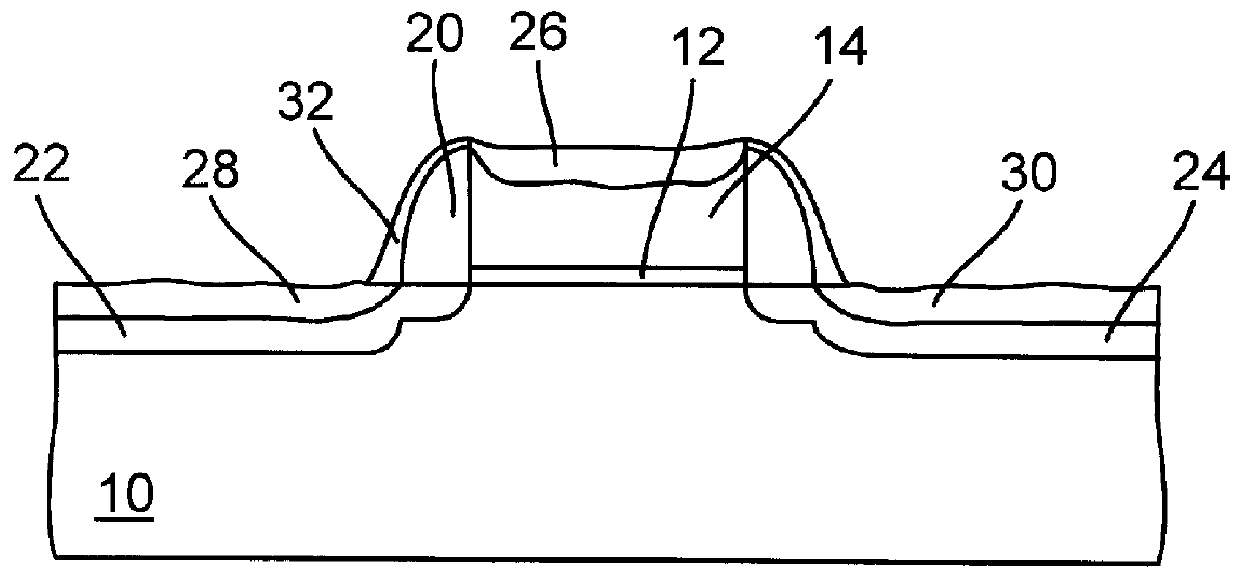
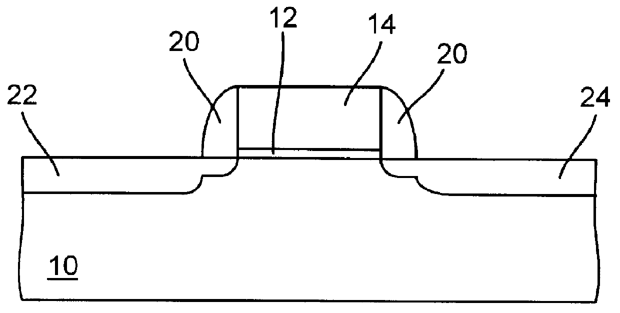
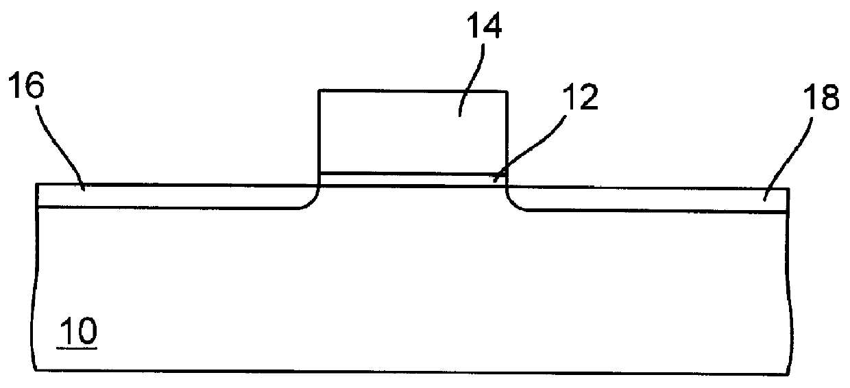
In one aspect, the present invention forms a semiconductor device including a polysilicon electrode over a substrate. Spacers are provided on either side of the polysilicon electrode, with upper edges of the spacers extending above an upper surface of the polysilicon electrode and upper recesses separating upper edges of the polysilicon electrode from the spacers. A metal layer is deposited over the polysilicon electrode, the spacers and the substrate, and the device is annealed to form a metal silicide layer on the polysilicon electrode and disposed between the spacers.

In another aspect, the present invention forms a semiconductor device including a polysilicon electrode over a substrate. Spacers are provided on either side of the polysilicon electrode, with lower edges of the spacers separated by a layer of insulating material from the substrate adjacent the polysilicon electrode and the lower edges of the spacers separated from the substrate by lower recesses along outer edges of...


PUM


Abstract

Silicidation of a polysilicon line having frcc upper sidewalls is performed so that no stress is applied to the sidewalls of the polysilicon line, resulting in the formation of a reduced stress silicide structure. This is accomplished by forming a polysilicon line having spacers on either side which extend above the upper surface of the polysilicon line but which are spaced from the edge of the polysilicon line. A layer of a metal such as titanium or tungsten is provided in contact with the top surface polysilicon line. The structure is annealed to cause the metal to react with the polysilicon to form a layer of silicide. Since the upper side portions of the polysilicon line are spaced away from the spacers during the silicidation anneal, the growing silicide region has room to expand without being subjected to lateral stresses in the silicidation process. The suicide is formed in a reduced stress condition, as compared to conventional processes, so that the silicide layer produced will be more readily converted to the desired low resistivity phase of silicide.

Description

1. Field of the InventionThe present invention relates to semiconductor devices incorporating electrodes consisting of a layer of polysilicon covered by a self-aligned layer of metal silicide.2. Description of the Related ArtAs line widths and geometries for semiconductor devices are made smaller, the polysilicon electrodes that form the gates of MOS devices and wiring lines within semiconductor devices become undesirably resistive. Multilayer electrodes in which a layer of polysilicon is covered by one or more layers of metals or metal silicides are used to provide electrodes having a lower resistance than electrodes consisting solely of polysilicon. Silicide electrodes may consist, for example, of a layer of polysilicon having a thickness of approximately 1000 .ANG. to 3000 .ANG. covered by titanium suicide or another metal silicide to a thickness of greater than 100 .ANG.. The silicide layer on the polysilicon layer acts as a lower resistance conduction path in parallel with the ...

Claims


Application Information

Patent Timeline
Patent Type & Authority Patents(United States)
IPC IPC(8): H01L21/336H01L21/02H01L21/28
CPCH01L21/28247H01L29/665H01L29/6656H01L29/6659H01L29/66545
Inventor LUR, WATERLIN, TONY
Owner UNITED MICROELECTRONICS CORP
Why Eureka
Try Eureka