Metal silicide alloy local interconnect

a technology of metal silicide alloy and local interconnection, which is applied in the direction of digital storage, semiconductor devices, instruments, etc., can solve the problems of complex wiring circuits, circuit design and processing technology challenges, and ca bars that do not provide a local interconnect solution

Inactive Publication Date: 2010-09-07
GLOBALFOUNDRIES INC
View PDF6 Cites 109 Cited by
  • Summary
  • Abstract
  • Description
  • Claims
  • Application Information

AI Technical Summary

Problems solved by technology

With continual scaling of semiconductor devices in each new generation, semiconductor technologies face challenges in circuit design and processing technology.
Circuits with complex wiring pose additional challenges since wiring of semiconductor devices is constrained by lithographic limitations.
Therefore, CA bars do not provide a local interconnect solution to a pair of conductive structures in the PC level or in the AA level that are separated by a distance longer than the horizontal dimensions of a CA bar.
Moreover, it is difficult to produce both circular shaped CA and oval shaped CA bar together due to the fact they require different illumination conditions during printing step and they have different etch bias during etch step.
In summary, prior art local interconnect methods between two conductive components within the PC level and the CA level have severe limitations in terms of the proximity between the two components.
Further, the prior art local interconnect methods also introduce parasitic capacitance between the local interconnect structure and other semiconductor components.
In the case of the exemplary prior art SRAM structure discussed above, the local interconnect structures that connect internal nodes, specifically the local interconnect structures that connects each of the pass gate transistors to the drains of one of the two pairs of a pull-up PFET and a pull-down NFET, occupies the M1 level, making utilization of the M1 level for bit line wiring impractical, and also increasing the parasitic capacitance of the internal nodes.

Method used


Image

  • Metal silicide alloy local interconnect
  • Metal silicide alloy local interconnect
  • Metal silicide alloy local interconnect

Examples


first embodiment

[0082]According to the present invention, a first photoresist 35 is applied to the top surface of the silicon containing layer 31 and lithographically patterned as shown in FIGS. 6A-6C. The pattern in the first photoresist 35 contains shapes for gate conductor lines to be formed subsequently. The pattern in the first photoresist 31 is transferred into the silicon containing layer 31 to form gate conductor lines 32. The pattern is further transferred into the gate dielectric 30 so that exposed portions of the gate dielectric 30 is etched from the top of the semiconductor substrate 10. The first photoresist 35 is subsequently removed. A suitable surface clean may be employed thereafter.

[0083]Alternate methods may be employed to form the gate conductor lines 31 such as methods according to a second embodiment of the present invention, which will be shown below after description of the common processing steps of the first and the second embodiments of the present invention.
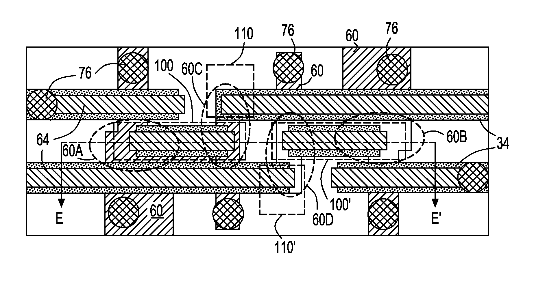
[0084]Accordi...

second embodiment

[0102]According to the present invention, the gate conductor lines 32 are formed using an alternate sequence of processing steps.

[0103]Referring to FIGS. 14A-14C, after the processing steps corresponding to FIG. 5, a first dielectric layer 51 is deposited directly on the silicon containing layer 31. The first dielectric layer 51 may comprise silicon oxide, silicon nitride, silicon oxynitride, or a silicon germanium alloy with a higher concentration of germanium than the underlying silicon containing layer 31. The thickness of the first dielectric layer 51 may be in the range from about 40 nm to about 300 nm, and is preferably in the range from about 80 nm to about 200 nm.

[0104]Referring to FIGS. 15A-15C, a third photoresist 53 is applied onto the top surface of the first dielectric layer 51 and is lithographically patterned. The pattern in the third photoresist 53 is transferred into the first dielectric layer 51 by a reactive ion etch (RIE), which is preferably selective to the und...


PUM

PropertyMeasurementUnit
thicknessaaaaaaaaaa
thicknessaaaaaaaaaa
thicknessaaaaaaaaaa

Abstract

A local interconnect is formed with a gate conductor line that has an exposed sidewall on an active area of a semiconductor substrate. The exposes sidewall comprises a silicon containing material that may form a silicide alloy upon silicidation. During a silicidation process, a gate conductor sidewall silicide alloy forms on the exposed sidewall of the gate conductor line and an active area silicide is formed on the active area. The two silicides are joined to provide an electrical connection between the active area and the gate conductor line. Multiple sidewalls may be exposed on the gate conductor line to make multiple connections to different active area silicides.

Description

FIELD OF THE INVENTION[0001]The present invention relates to semiconductor structures, and particularly to semiconductor structures with a local interconnect formed with metal silicide alloys and methods of manufacturing the same.BACKGROUND OF THE INVENTION[0002]With continual scaling of semiconductor devices in each new generation, semiconductor technologies face challenges in circuit design and processing technology. Circuits with complex wiring pose additional challenges since wiring of semiconductor devices is constrained by lithographic limitations.[0003]For example, conventional static random access memory (SRAM) devices require complex wiring even at an M1 level (the first metal wiring level above a semiconductor substrate) since the internal nodes of an SRAM cell need to be connected at the M1 level. The use of the M1 level for internal node wiring forces the wiring of the bit lines into an M2 level (the second wiring level above the semiconductor substrate) and the wiring o...

Claims


Application Information

Patent Timeline
Patent Type & Authority Patents(United States)
IPC IPC(8): H01L27/10G11C11/00G11C11/34H01L27/11G11C5/06
CPCG11C11/412H01L21/76895H01L27/11H01L27/1104Y10S257/903H10B10/00H10B10/12
Inventor WANN, CLEMENT H.YANG, HAINING S.
Owner GLOBALFOUNDRIES INC
Why Eureka
Try Eureka