FET gate structure with metal gate electrode and silicide contact

a gate electrode and metal gate electrode technology, applied in the direction of semiconductor/solid-state device details, instruments, transistors, etc., can solve the problems of poly depletion effect, increase of gate leakage current and diffusion of dopants, and manufacturing problems

Active Publication Date: 2006-06-06
GLOBALFOUNDRIES U S INC
View PDF18 Cites 95 Cited by
  • Summary
  • Abstract
  • Description
  • Claims
  • Application Information

AI Technical Summary

Problems solved by technology

With the continued scaling of CMOS devices to smaller dimensions, the gate dielectrics of these devices have been reduced to thicknesses well below 20 Å. This in turn has led to greatly increased gate leakage currents and diffusion of dopants from the polysilicon gate structures (often referred to as the poly depletion effect).
This approach may present manufacturing problems in two ways.
First, a very narrow gate structure (corresponding to a very short channel length, perhaps less than 70 nm) results in a high-aspect-ratio trench which may be difficult to fill without introducing a void in the metal.
Second, a metal planarization process (typically chemical-mechanical polishing or CMP) is susceptible to dishing effects which cause nonuniformities in the metal thickness (and thus in the height of the metal gate).

Method used


Image

  • FET gate structure with metal gate electrode and silicide contact
  • FET gate structure with metal gate electrode and silicide contact
  • FET gate structure with metal gate electrode and silicide contact

Examples


first embodiment

[0032] Single-metal Replacement Gate

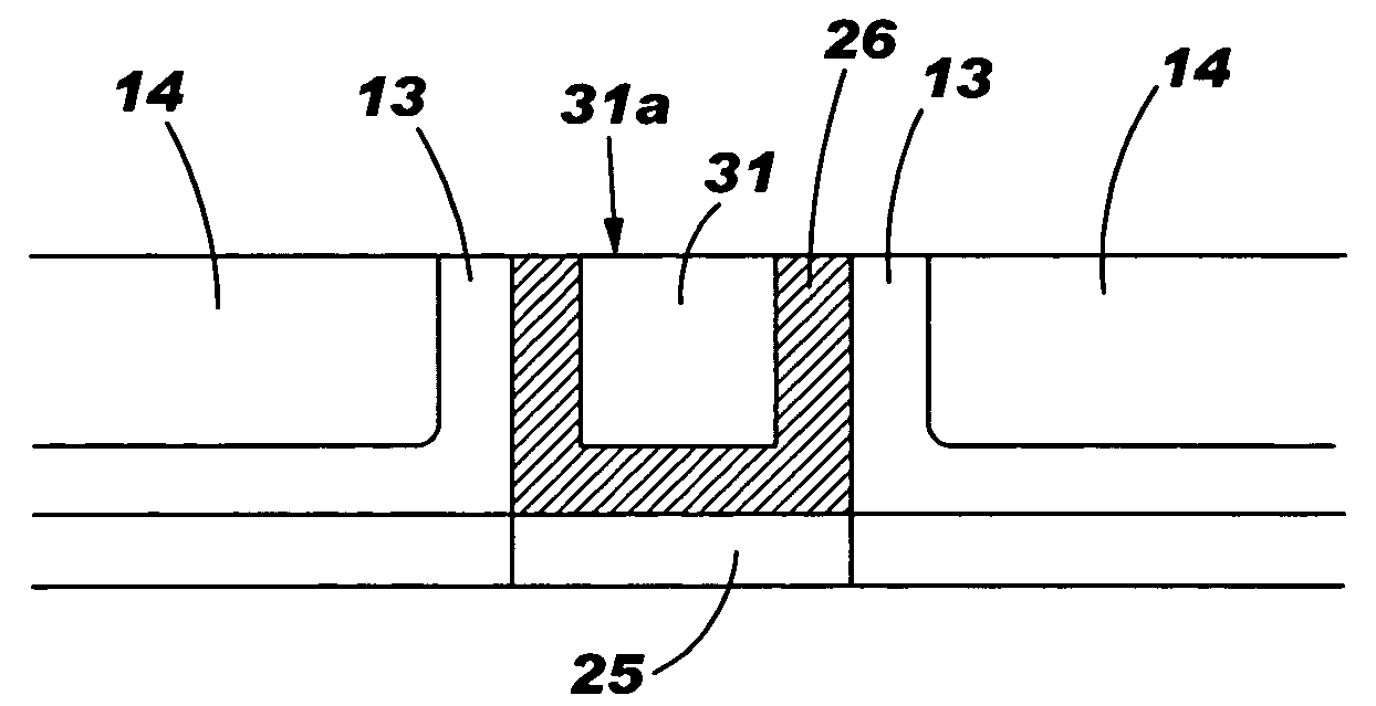
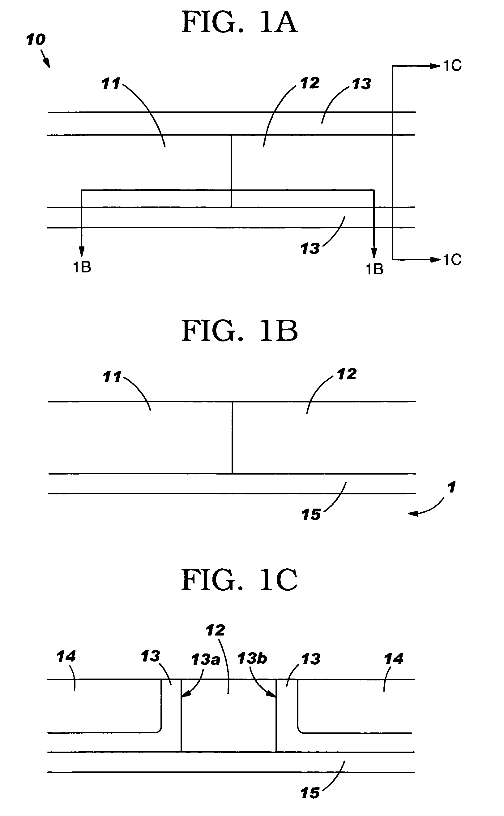
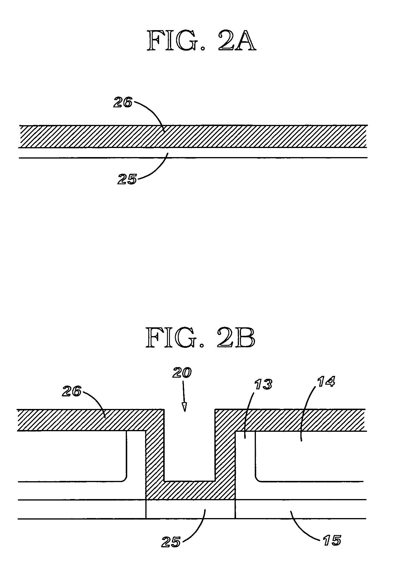
[0033]In this embodiment, the dummy polysilicon gate structures 11, 12 are removed in the same process; any convenient process having selectivity to nitride 13 and oxide 14 may be used. This process exposes the sacrificial oxide layer 15, which is then also removed. A trench 20 is thus formed with sidewalls 13a, 13b of nitride and an exposed portion of substrate 1 on the bottom. A new gate dielectric 25 is formed on the exposed substrate, either by a deposition process or a thermal growth process. A conformal layer of metal 26 is then deposited as a blanket layer, covering the sidewalls of the trench and the gate dielectric 25. The composition and thickness of layer 26 are chosen to provide the desired work function, as is understood by those skilled in the art. FIGS. 2A and 2B are longitudinal and transverse cross-section views, respectively, of the structure after metal layer 26 is deposited.

[0034]A blanket layer 31 of undoped polycrystalline or...

second embodiment

[0037] Dual-metal Replacement Gate

[0038]In this embodiment, the dummy p+ and n+ polysilicon gate structures are removed separately, which requires masking of the polysilicon structure not being removed. FIG. 6 shows the structure after masking the p+ dummy gate 11, removing the n+ dummy gate 12 and the underlying sacrificial gate oxide 15, and stripping the mask. A portion of the substrate 1 is thereby exposed. A blanket gate dielectric layer 75 is then grown or deposited, and a blanket metal layer 75 is deposited thereover (see FIG. 7).

[0039]A blanket layer 81 of undoped polycrystalline or amorphous silicon is then deposited over layer 26. As in the first embodiment, the composition of layer 81 is chosen to provide the optimum trench fill. The structure is then planarized to again expose dummy gate 11, so that the top surface 81a of the fill material 81 is coplanar therewith. The planarization process may be performed in a single step, e.g. CMP of the poly / amorphous silicon, contin...


PUM

PropertyMeasurementUnit
channel lengthaaaaaaaaaa
thicknessesaaaaaaaaaa
electrical performanceaaaaaaaaaa

Abstract

A method is provided for fabricating a single-metal or dual metal replacement gate structure for a semiconductor device; the structure includes a silicide contact to the gate region. A dummy gate structure and sacrificial gate dielectric are removed to expose a portion of the substrate; a gate dielectric is formed thereon. A metal layer is formed overlying the gate dielectric and the dielectric material. This metal layer may conveniently be a blanket metal layer covering a device wafer. A silicon layer is then formed overlying the metal layer; this layer may also be a blanket wafer. A planarization or etchback process is then performed, so that the top surface of the dielectric material is exposed while other portions of the metal layer and the silicon layer remain in the gate region and have surfaces coplanar with the top surface of the dielectric material. A silicide contact is then formed which is in contact with the metal layer in the gate region.

Description

[0001]This application is related to application Ser. No. 10 / 707,759, “Method of forming FET silicide gate structures incorporating inner spacers,” filed the same day and assigned to the same assignee as the present application. The disclosure of the above-noted application is incorporated herein by reference.BACKGROUND OF INVENTION[0002]This invention relates to the manufacture of advanced semiconductor devices, particularly advanced CMOS integrated devices in which metal gate electrodes are used.[0003]With the continued scaling of CMOS devices to smaller dimensions, the gate dielectrics of these devices have been reduced to thicknesses well below 20 Å. This in turn has led to greatly increased gate leakage currents and diffusion of dopants from the polysilicon gate structures (often referred to as the poly depletion effect).[0004]Metal gates are now being used to mitigate the poly depletion effect and control the leakage current, and thus to ensure electrical performance in highly...

Claims


Application Information

Patent Timeline
Patent Type & Authority Patents(United States)
IPC IPC(8): H01L21/336H01L29/76H01L21/28H01L21/3205H01L21/335H01L21/8238H01L27/092H01L29/423H01L29/49H01L29/78
CPCH01L21/28079H01L21/28247H01L29/66583H01L29/66545H01L21/823835G01R1/06711G01R1/07342G01R1/0735G01R31/2601
Inventor KU, VICTORSTEEGEN, ANWANN, HSING-JEN C.
Owner GLOBALFOUNDRIES U S INC
Why Eureka
Try Eureka