Nonvolatile memory device for preventing bitline high voltage from discharge

a nonvolatile memory and high voltage technology, applied in the direction of digital storage, instruments, transistors, etc., can solve the problems of undesirable reduction of high voltage, inability to program operation, and high voltage to be forwarded

Active Publication Date: 2007-02-06
SAMSUNG ELECTRONICS CO LTD
View PDF4 Cites 20 Cited by
  • Summary
  • Abstract
  • Description
  • Claims
  • Application Information

AI Technical Summary

Problems solved by technology

This may cause a programming operation instability, which forces a memory cell that should be in an erase state to be programmed.
However, undesirable leakage currents may still be generated in the layout structure with narrower bitline pitches that cause a high voltage to be forwarded into the low voltage field.
If a distance between a DC (Direct Contact) contact in the high voltage field and a bitline in the low voltage field is narrow, it may occur with an undesirable effect such as an oxide breakdown or a high voltage leakage between the high and low voltage fields when there have been misalignments or micro-bridges during a manufacturing process.
The defective results arise from the fact that an electric field is enlarged in accordance with a narrower distance between the high and low voltage fields.
This mechanism may cause undesirable reduction of the high voltage during an erase operation.
Such a decrease of the high voltage applied to the bulk of the memory cells during an erase operation acts as a leading factor declining product yields and reliabilities.
However, if the pitch (or distance) between the bitlines isolated from each other on the layout arrangement are narrow, undesirable leakage currents may occur resulting in a high voltage surge into the low-voltage field.
Because short distances exist between DC contacts of the high voltage field and bitlines of the low voltage field, an oxide breakdown or a high voltage discharge may occur between the high and low voltage fields during an erase operation if there are any misalignments or micro-bridges present from the manufacturing process.
This drop of high voltage during an erase operation is a significant factor contributing to the degradation in operational reliability of the flash memory device.

Method used


Image

  • Nonvolatile memory device for preventing bitline high voltage from discharge
  • Nonvolatile memory device for preventing bitline high voltage from discharge
  • Nonvolatile memory device for preventing bitline high voltage from discharge

Examples


Embodiment Construction

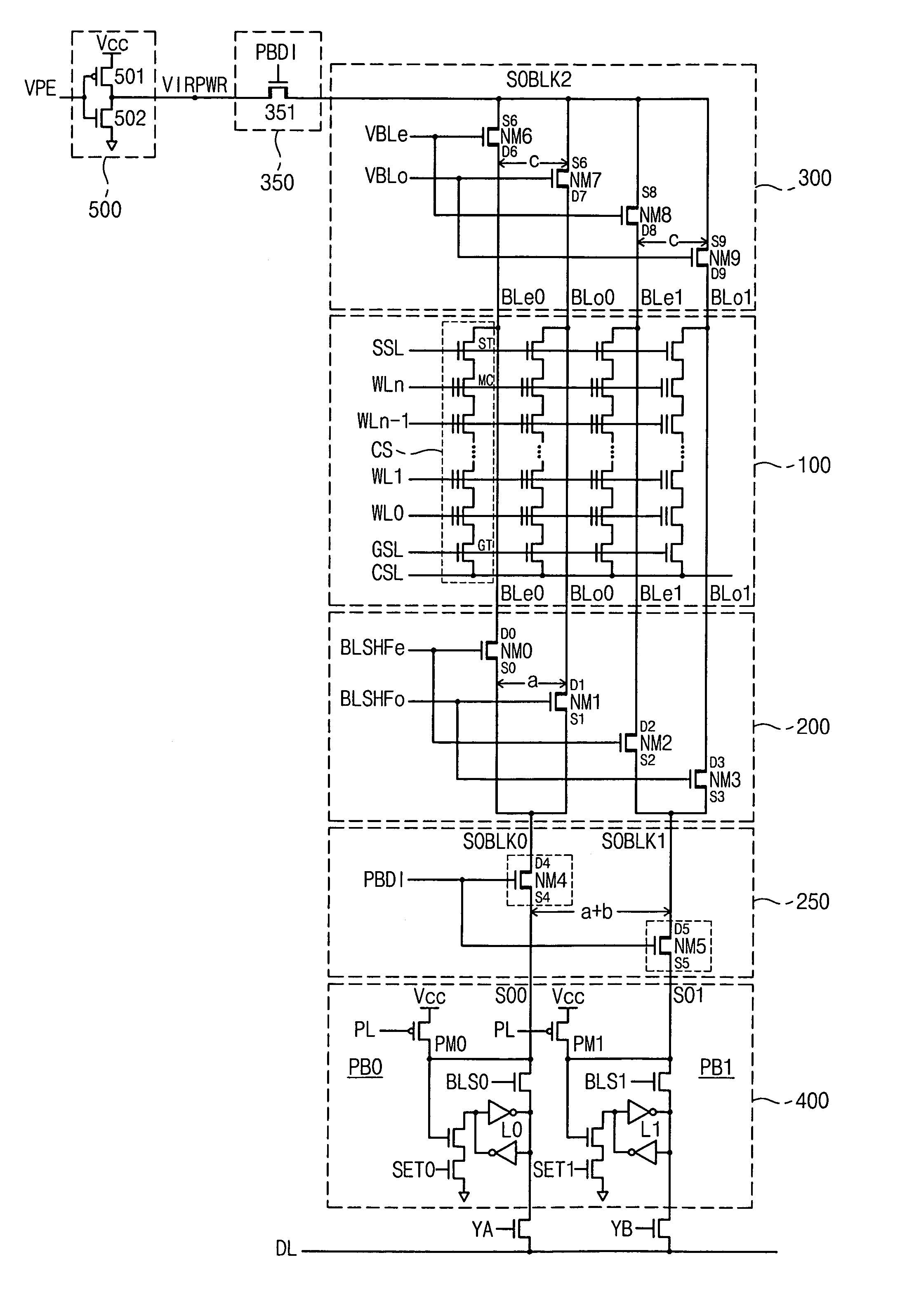
[0034]Preferred embodiments of the invention will now be described below in more detail with reference to the accompanying drawings. The invention may, however, be embodied in different forms and should not be constructed as limited to the embodiments set forth herein. Rather, these embodiments are provided so that this disclosure will be thorough and complete, and will fully convey the scope of the invention to those skilled in the art. Like numerals refer to like elements throughout the specification.

[0035]Some embodiments of the invention are applicable to NAND flash memory devices having a memory cell array constructed of a number of cell strings, each cell string including a number of memory cells connected in series between a string selection transistor and a ground selection transistor. Some embodiments of the invention are applicable to NAND flash memory devices that use high voltages for an erase operation. According to some embodiments of the invention, an erase operation ...


PUM


Abstract

According to some embodiments, a nonvolatile semiconductor memory device includes high voltage circuits that prevent high voltages, which are applied to bitlines during an erase operation, from being applied to low voltage circuits that are operable with low voltages. Each high voltage circuit includes a first switching circuit for selectively isolating the low voltage circuit from the bitlines, and a second switching circuit for inhibiting a leakage current to the low voltage circuit from the bitlines. The second switching circuit is connected between the first switching circuit and the low voltage circuit.

Description

CROSS-REFERENCE TO RELATED APPLICATIONS[0001]This patent application claims priority from Korean Patent Application 2003-86373, filed on 1 Dec. 2003, the content of which is hereby incorporated by reference in its entirety for all purposes.BACKGROUND OF THE INVENTION[0002]1. Field of the Invention[0003]This disclosure relates to a nonvolatile memory device, and more particularly, to a nonvolatile memory device that prevents a high voltage of a bitline from being discharged.[0004]2. Description of the Related Art[0005]Electrically-Erasable Programmable Read-Only Memories (EEPROMs) and flash EEPROMs, or flash memories, are convenient in that data can be electrically reprogrammable after erasing previous data is erased. Thus, they are widely used today. NAND flash memories are especially advantageous to achieving high integration densities relative to other commercial flash memories.[0006]In general, a NAND flash memory has a cell array that includes a number of cell strings, each cell...

Claims


Application Information

Patent Timeline
Patent Type & Authority Patents(United States)
IPC IPC(8): G11C16/04G11C16/06G11C5/06G11C16/14G11C16/24H01L21/8247H01L27/115H01L29/788H01L29/792
CPCG11C16/24G11C16/0483G11C16/14
Inventor CHO, HYUN-CHULLEE, YEONG-TAEK
Owner SAMSUNG ELECTRONICS CO LTD
Why Eureka
Try Eureka