Novel capping structure for enhancing dR/R of the MTJ device

a capping structure and enhancing technology, applied in the field of capping layers, can solve problems such as hayashi's inability to teach, and achieve the effect of well controlled magnetization and switching characteristics

Inactive Publication Date: 2005-12-15
HEADWAY TECH INC +1
View PDF31 Cites 177 Cited by
  • Summary
  • Abstract
  • Description
  • Claims
  • Application Information

AI Technical Summary

Benefits of technology

The patent aims to create a free layer in an MTJ element that has controlled magnetization and switching characteristics. This results in an R-H curve that does not have any kinks or vortexes.

Problems solved by technology

The technical problem addressed in this patent text is to improve the performance of a magnetic tunnel junction (MTJ) element in a magnetic read head or a magnetic sensor. The text describes various layers and their functions in the MTJ element, including the pinned layer, the AFM layer, the tunnel barrier layer, and the free layer. The text also discusses the importance of the magnetostriction and coercivity of the free layer. The text emphasizes the need for a thicker mag layer to achieve a high MR ratio and low λS value for advanced MRAM technologies. The text also describes the use of a capping layer to protect the layers and function as an electrical contact. The text describes various layers and their functions in the MTJ element.

Method used


Image

  • Novel capping structure for enhancing dR/R of the MTJ device
  • Novel capping structure for enhancing dR/R of the MTJ device
  • Novel capping structure for enhancing dR/R of the MTJ device

Examples


first embodiment

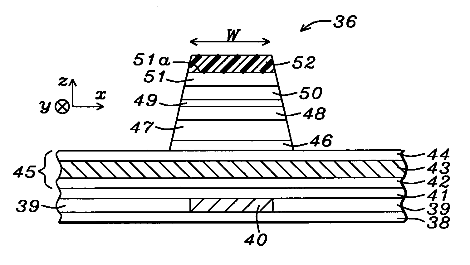
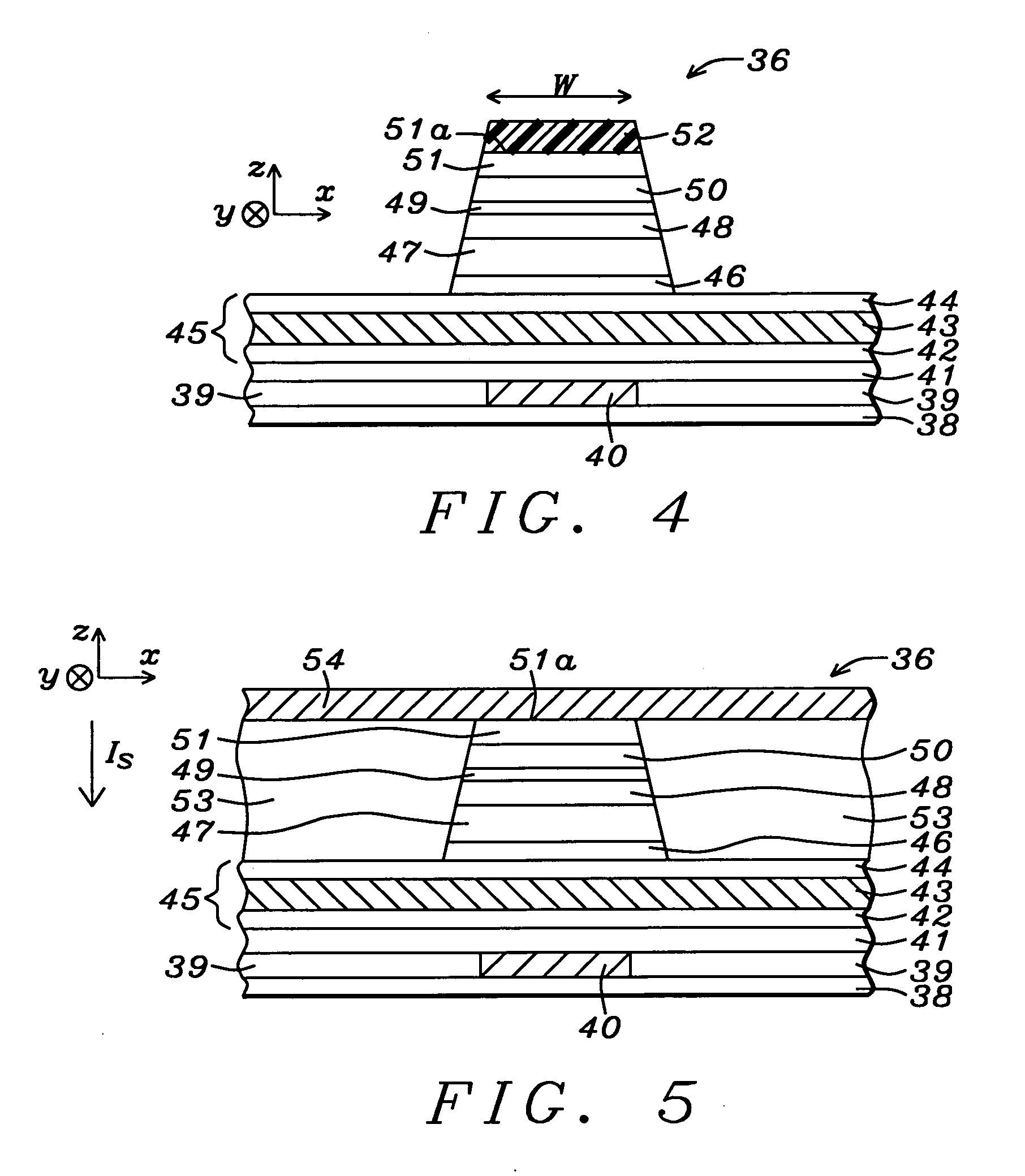
[0028] An MRAM structure formed according to the present invention will now be described. Referring to FIG. 4, a partially completed MRAM structure 36 is shown that includes a substrate 38 which may be silicon or another semiconductor substrate used in the art that typically contains other devices such as transistors and diodes. A first insulation layer 39 comprised of Al2O3, silicon oxide, or the like is disposed on the substrate 38. There is a first conductive line comprised of copper, for example, formed within and coplanar with the first insulation layer 39. For the purpose of this discussion, the first conductive line is a word line 40 that is used to conduct current in a +y or −y direction. Optionally, the first conductive line may be called a digit line, data line, row line, or column line as appreciated by those skilled in the art. The word line 40 may be enclosed on the sides and bottom by a thin diffusion barrier layer (not shown). There is a second insulation layer 41 suc...

second embodiment

[0053] In a second embodiment depicted in FIG. 7, a magnetoresistive (TMR) read head 60 is shown in which an MTJ element is formed between a bottom (S1) shield 62 and an upper (S2) shield 75. A composite capping layer is formed on a moderate spin polarization layer such as a NiFe(17.5%) free layer in the MTJ to enhance dR / R and provide acceptable magnetostriction.

[0054] A substrate 62 is provided that may be a bottom shield comprised of NiFe in the TMR read head 60 as is understood by those skilled in the art. A shield capping layer 64 is formed on the bottom shield 62 by a previously described method that involves sequentially depositing a Ta layer with a thickness of about 50 to 80 Angstroms and a Ru layer with a thickness of between 20 and 30 Angstroms on the bottom shield 62. Thereafter, the Ru layer is removed by a sputter etch process that also partially removes the underlying Ta layer to form an amorphous Ta layer as the shield capping layer 64. The shield capping layer 64 ha...


PUM


Abstract

An MTJ in an MRAM array or in a TMR read head is comprised of a capping layer with a lower inter-diffusion barrier layer, an intermediate oxygen gettering layer, and an upper metal layer that contacts a top conductor. The composite capping layer is especially useful with a moderate spin polarization free layer such as a NiFe layer with a Fe content of about 17.5 to 20 atomic %. The capping layer preferably has a Ru/Ta/Ru configuration in which the lower Ru layer is about 10 to 30 Angstroms thick and the Ta layer is about 30 Angstroms thick. As a result, a high dR/R of about 40% is achieved with low magnetostriction less than about 1.0 E-6 in an MTJ in an MRAM array. Best results are obtained with an AlOx tunnel barrier layer formed by an in-situ ROX process on an 8 to 10 Angstrom thick Al layer.

Description


Claims


Application Information

Patent Timeline
Owner HEADWAY TECH INC
Why Eureka
Try Eureka