Semiconductor memory device

a memory device and semiconductor technology, applied in the field of semiconductor memory devices, can solve the problems of increasing the difficulty of setting the reference current or the reference voltage, the inability to provide appropriate reference current or reference voltage, and the inability to perform readings, etc., and achieve the effect of low cos

Inactive Publication Date: 2005-12-15
XENOGENIC DEV LLC
View PDF5 Cites 41 Cited by
  • Summary
  • Abstract
  • Description
  • Claims
  • Application Information

AI Technical Summary

Benefits of technology

The semiconductor memory device described in this patent reduces costs by reducing the space needed for certain components called reference current generation circuits. This allows for more efficient use of resources during production.

Problems solved by technology

The technical problem addressed in this patent text relates to improving the accuracy of detecting the memory cell's resistance value during Read Off mode operations in a data line driver and Amplifier. Due to variations in the resistance value of the memory cells, the leak current may affect the detection of the memory cell's resistance value, making it hard to determine the correct reference current or reference voltage needed for accurately measuring the resistance value. This issue needs to be solved to ensure accurate measurement of the memory cell's resistance without being affected by the leak current direction.

Method used


Image

  • Semiconductor memory device
  • Semiconductor memory device
  • Semiconductor memory device

Examples


second embodiment

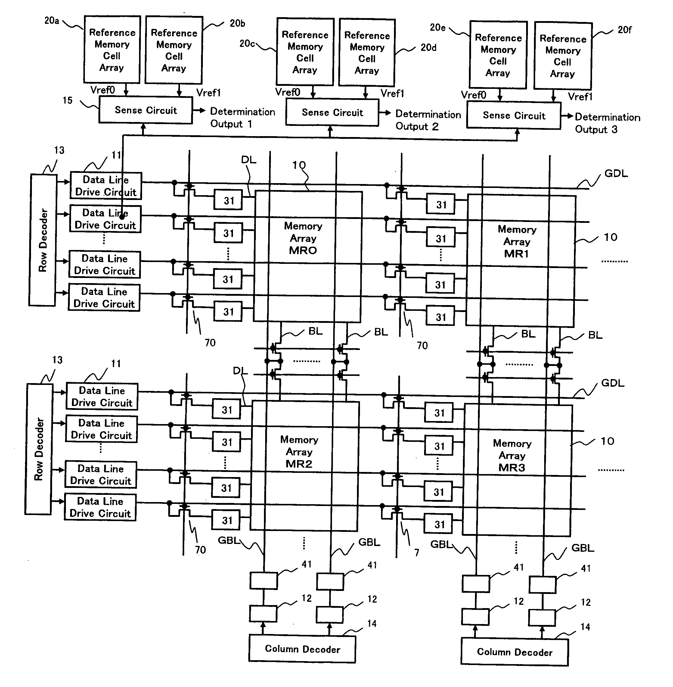
[0132] Although a description was made of a case where when the 4-level data of one memory cell is read out by selecting one data line from a selected memory cell array, the three sense circuits 15 are used in parallel to compare its voltage level with three reference levels at the same time according to the first embodiment as shown in FIG. 1, according to this embodiment, a description will be made of a case where one sense circuit 15 is used to change over three reference levels in terms of time in rotation.

[0133] According to the readout method in the first embodiment, as shown in FIG. 25, the middle current level between the upper limit value of the readout current of the high resistance memory cell generated in the reference memory cell array when the high resistance memory cell is selected, and the lower limit value of the readout current of the low resistance memory cell generated in the reference memory cell array when the low resistance memory cell is selected is generate...


PUM


Abstract

In a semiconductor memory device having a crosspoint-type memory cell array, each reference level between two adjacent memory levels when memory levels of multi-level information stored in a memory cell are arranged in order of size of resistance values of a corresponding variable resistive element is defined by a reference current in a middle state between a first and a second current states. In the first current state, a readout current of high resistance selected cell in which the resistance is higher in the two adjacent memory levels becomes the largest state depending on a distribution pattern of a resistance state of the other unselected cell. In the second current state, a readout current of low resistance selected cell in which the resistance is lower in the two adjacent memory levels becomes a smallest state depending on a distribution pattern of a resistance state of the other unselected memory cell.

Description


Claims


Application Information

Patent Timeline
Owner XENOGENIC DEV LLC
Why Eureka
Try Eureka