

Photosemiconductor device
- Summary
- Abstract
- Description
- Claims
- Application Information
AI Technical Summary
Benefits of technology
Problems solved by technology
Method used
Image

Examples
Embodiment Construction
Principle of the Present Invention
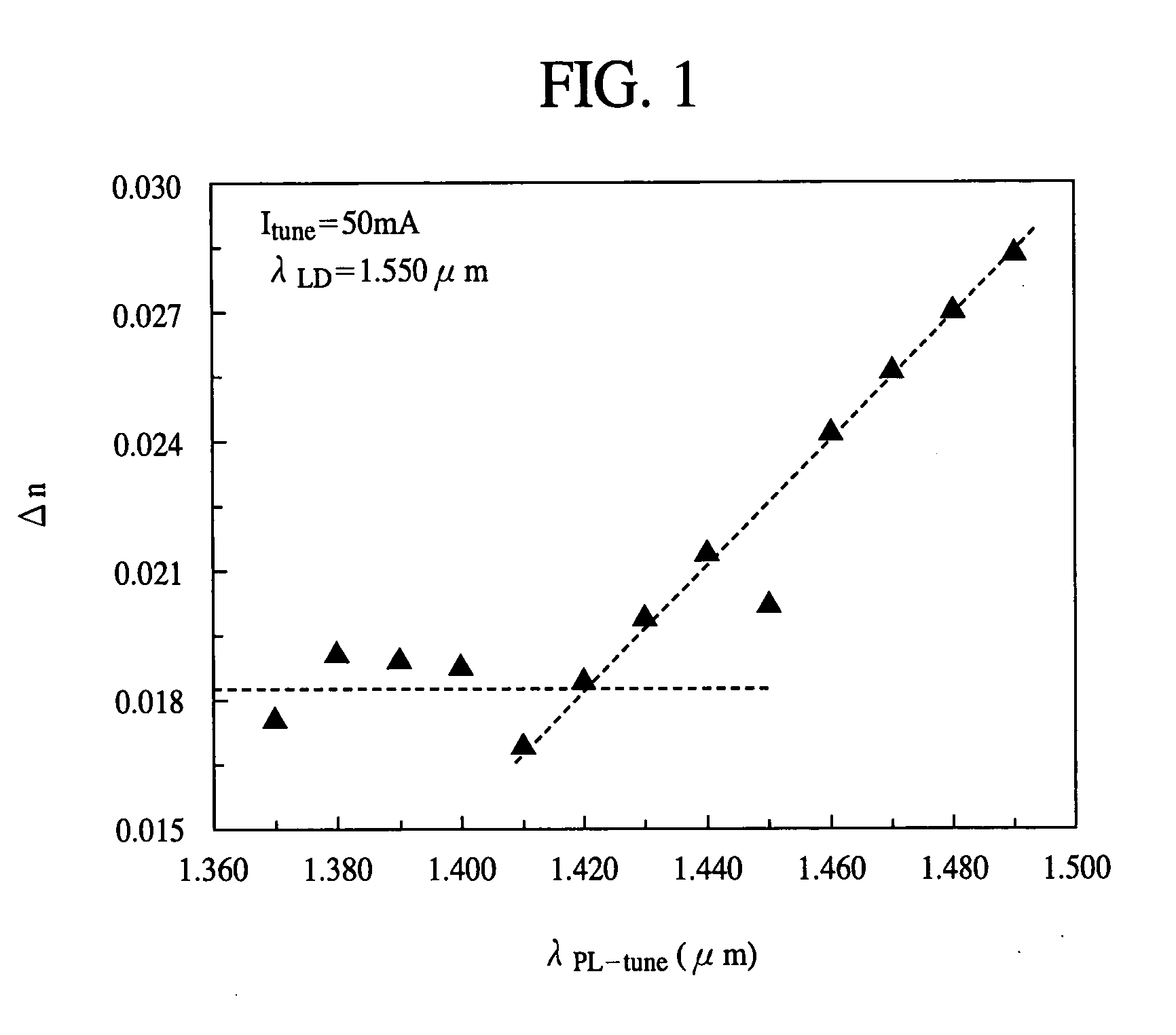
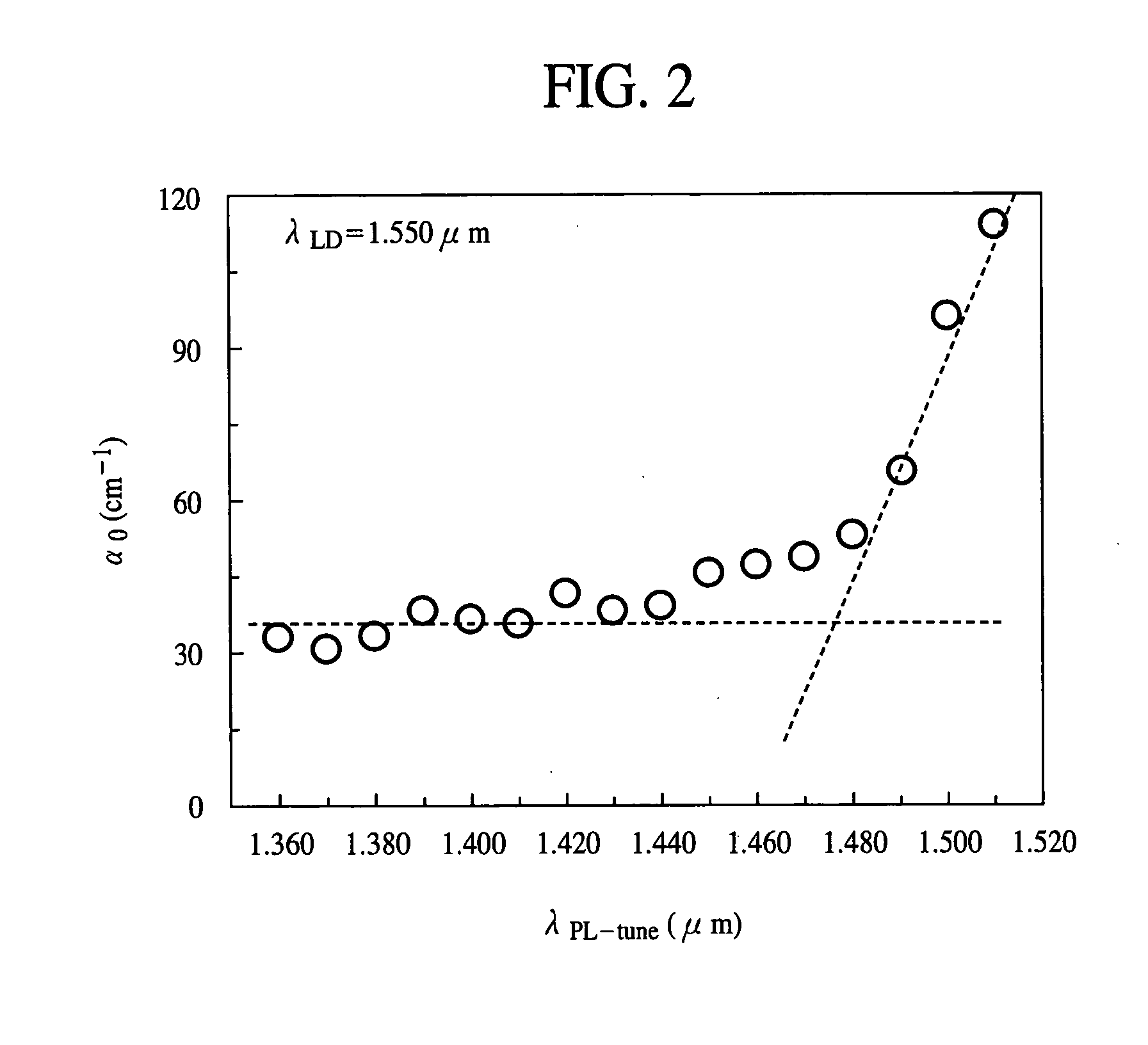
[0037] First, the principle of the present invention will be explained with reference to FIGS. 1 and 2. FIG. 1 is a graph of the dependency of the refractive index change An of the refractive index control layer on the effective forbidden bandwidth of the refractive index control layer. FIG. 2 is a graph of the dependency of the fundamental absorption α0 of the refractive index control layer on the effective forbidden band of the refractive index control layer.
[0038] The inventors of the present application have made earnest studies of the refractive index control layer having the refractive index changed by current injection, which is used as the wavelength control layers, etc. of the variable wavelength lasers, such as TTG-DFB-LD, etc. so as to realize a refractive index control layer having a small fundamental absorption with respect to light-to-be-controlled which propagates through an optical waveguide including the refractive index control l...
PUM
 Abstract
Description
Claims
Application Information