Stretchable crystalline semiconductor nanowire and preparation method thereof

A technology of nanowires and semiconductors, applied in the field of spring structure crystal nanowires, can solve the problems of the existing technology, such as not being very good, achieve the effect of convenient integration and use, and improve device characteristics and stability

Active Publication Date: 2019-01-18
NANJING UNIV
View PDF6 Cites 11 Cited by
  • Summary
  • Abstract
  • Description
  • Claims
  • Application Information

AI Technical Summary

Problems solved by technology

[0007] The growth of materials with stretchable crystalline nanowire spring structure is the basis of flexible and stretchable electronic devices, and the existing technology does not have a good way to solve it

Method used


Image

  • Stretchable crystalline semiconductor nanowire and preparation method thereof
  • Stretchable crystalline semiconductor nanowire and preparation method thereof
  • Stretchable crystalline semiconductor nanowire and preparation method thereof

Examples


Embodiment Construction

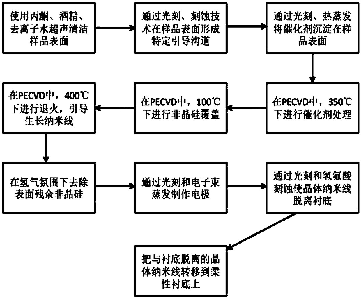
[0041] In order to make the purpose, technical solution, function and advantages of the present invention more clear, the present invention will be further explained in detail below in conjunction with specific examples.

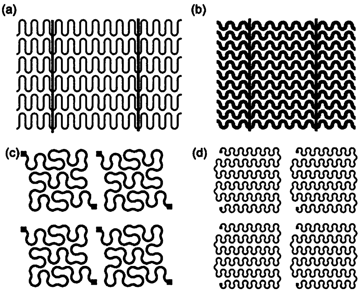
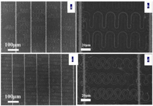
[0042] Such as figure 2 As shown, the present invention provides a stretchable crystalline semiconductor nanowire having an elongated body. The stretchable crystalline semiconductor nanowire has a curved structure and has a plurality of stretchable units in the axial direction, and the plurality of stretchable units are connected in sequence to form a stretchable crystalline semiconductor nanowire.

[0043] Further, the diameter of the nanowire is between 20-200 nanometers, and the nanowire is a crystalline inorganic semiconductor structure.

[0044] Such as figure 2As shown, the schematic diagram of the crystal nanowire array design, in which the blue (dark) area is the catalyst area (a) (b) (c) (d) respectively represent four different spring-shaped cu...


PUM

PropertyMeasurementUnit
diameteraaaaaaaaaa
thicknessaaaaaaaaaa
diameteraaaaaaaaaa

Abstract

The invention relates to a stretchable crystalline semiconductor nanowire and a preparation method thereof. The stretchable crystalline semiconductor nanowire comprises a long and thin main body, thediameter of the nanowire is 20-200 nm, and the nanowire is of a crystalline inorganic semiconductor structure. The stretchable crystalline semiconductor nanowire is of a bending structure and is provided with multiple stretchable units in the axial direction, the multiple stretchable units are connected in sequence, and therefore, the stretchable crystalline semiconductor nanowire is formed. Withthe adoption of IP-SLS and other methods, the channel step guided nanowire grows in PECVD, and a spring-structured crystalline nanowire array is manufactured with a modern micro-machining technology.The nanowire and guide channel sections can be effectively adjusted, so that the nanowire can be further peeled and transferred to other flexible substrates. The method for preparing the spring-structured crystalline nanowire has broad prospects in the fields of flexible electronics and sensors.

Description

[0001] priority statement [0002] This application is a partial continuation of CN201710450420.3 (publication number CN107460542A) submitted on June 15, 2017, and claims its priority, the entire content of which is hereby incorporated by reference. technical field [0003] The invention relates to the field of flexible and stretchable electronics and devices, and relates to a method for making spring structure crystal nanowires with flexible and stretchable properties by using channel-guided planar nanowire growth technology on a substrate and through micromachining technology . Especially the method of channel-guided self-positioning self-directed growth, transfer, and electrical integration of planar semiconductor nanowires to prepare spring-structure crystal nanowires. Background technique [0004] With the development of the contemporary electronic display industry, flexible and stretchable electronic devices (especially display devices) play an increasingly important ...

Claims


Application Information

Patent Timeline
Patent Type & Authority Applications(China)
IPC IPC(8): C30B25/18C30B29/06C30B29/08C30B29/40C30B29/60
CPCC30B25/183C30B25/186C30B29/06C30B29/08C30B29/406C30B29/60B82Y10/00B82Y40/00H01L21/02381H01L21/02422H01L21/0243H01L21/02532H01L21/02546H01L21/02587H01L21/02592H01L21/02603H01L21/02639H01L21/02645H01L21/02653H01L29/0673H01L29/775C30B29/42H01L21/02598H01L21/02658H01L29/0669
Inventor 余林蔚薛兆国董泰阁王军转
Owner NANJING UNIV
Why Eureka
Try Eureka