Method of preparing three-dimensional super-stretchable crystalline nanowire

A nanowire and crystalline technology, applied in the field of preparation of three-dimensional ultra-stretchable crystalline nanowires, can solve the problems of relaxation space reduction, limitation, nanowire breakage, etc., achieve more relaxation space, improve stretchability Stretchability, the effect of good stretchability

Active Publication Date: 2020-02-07
NANJING UNIV
View PDF6 Cites 5 Cited by
  • Summary
  • Abstract
  • Description
  • Claims
  • Application Information

AI Technical Summary

Problems solved by technology

[0003] However, the natural rigidity of many materials severely limits the emerging new flexible and stretchable electronic devices. Therefore, it is very important to control the morphology of crystalline nanowires to make them super stretchable.
Since the planar crystalline nanowires are greatly constrained by the substrate, the relaxation space is reduced, and it is very easy to cause the nanowires to be broken during the stretching process, making it difficult to prepare reliable flexible electronic devices.

Method used


Image

  • Method of preparing three-dimensional super-stretchable crystalline nanowire
  • Method of preparing three-dimensional super-stretchable crystalline nanowire
  • Method of preparing three-dimensional super-stretchable crystalline nanowire

Examples


Embodiment Construction

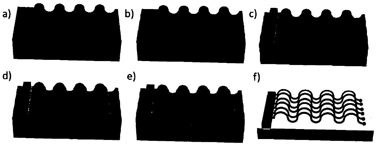
[0027] In order to make the technical solutions and advantages of the present invention clearer, the present invention will be further elaborated below in conjunction with specific implementation examples. The flow chart is as follows figure 1 shown.

[0028] The steps are as follows: 1) Use silicon wafers, glass, aluminum foil, compounds (such as silicon nitride, silicon oxide, silicon oxynitride), polymers or other metal materials as substrates, and use PECVD or PVD processes to deposit on the substrates An insulating dielectric layer (about 4 μm); 2) Use photolithography, electron beam direct writing or mask technology to define the pattern of the step edge, use inductively coupled plasma (ICP) etching or reactive plasma etching (RIE) The process etches the dielectric layer to form a vertical step sidewall (about 1 μm depth); use ICP or RIE alternate cycle etching method to etch the step structure; first use C in the etching process 4 f 8 、CF 4 , SF 6 Reactive gases wit...


PUM


Abstract

The invention relates to a method of preparing a three-dimensional super-stretchable crystalline nanowire, which comprises the following steps of: (1) depositing an insulating dielectric layer on a substrate as a sacrificial layer by using PECVD or PVD, (2) defining a periodic step edge pattern by using photoetching and electron beam direct writing, and etching the dielectric layer by using a drymethod or wet method alternate etching process to form vertical step side walls, 3) treating the surface of the step with corrosive liquid to form a wavy step, 4) defining a pattern vertical to the step by photoetching electron beam direct writing or a mask plate technology again, and preparing a secondary guide channel vertical to the step by an etching technology, 5) locally depositing a strip-shaped catalytic metal layer through a photoetching, evaporation or sputtering process, (6) converting the catalytic metal layer into separated metal nanoparticles, and (7) reducing the temperature tobe lower than the melting point of the catalytic metal particles, depositing and covering an amorphous semiconductor precursor film layer on the surface of the whole structure, depositing crystallinenanowires, and enabling the nanowires to grow along the guide channel of a wavy step.

Description

technical field [0001] The invention relates to a method for obtaining super-stretchable crystalline nanowires (nanowire) by channel guiding technology, in particular to a method for forming large-area, easy-to-locate wave-shaped guiding channels by using two etching processes. Background technique [0002] Semiconductor crystalline silicon nanowire (Nanowire) is the core material of modern microelectronics technology due to its high carrier mobility and the ability to achieve efficient, stable and reliable doping processes. Here, the inventor of the present application is the earliest A planar solid-liquid-solid (IP SLS) growth mode is proposed, in which amorphous silicon is used as a precursor, and crystalline silicon nanowire structures are grown by absorbing amorphous silicon with low melting point metal indium and tin nanoparticles. At the same time, three-dimensional nano-steps can be prepared by using two-time etching technology, and the steps are used as a guide. The...

Claims


Application Information

Patent Timeline
Patent Type & Authority Applications(China)
IPC IPC(8): H01L21/02B82Y40/00
CPCH01L21/02532H01L21/02603H01L21/02592H01L21/0262H01L21/02672B82Y40/00
Inventor 余林蔚孙莹董泰阁王军转
Owner NANJING UNIV
Why Eureka
Try Eureka