Method for fabricating semiconductor device

a memory device and semiconductor technology, applied in the direction of semiconductor devices, basic electric elements, electrical appliances, etc., can solve the problems of reducing and increasing the threshold voltage change, so as to prevent the decrease of the charge mobility of the transistor and improve the device characteristi

Inactive Publication Date: 2008-04-03
SK HYNIX INC
View PDF3 Cites 11 Cited by
  • Summary
  • Abstract
  • Description
  • Claims
  • Application Information

AI Technical Summary

Benefits of technology

[0018]The present invention contemplates a method for fabricating a semiconductor device to improve device characteristic by preventing a decrease in charge mobility of a transistor due to compressive stress exerted to a transistor from a thin layer formed over a memory cell and a transistor.

Problems solved by technology

However, when the silicon nitride layer used as the stopping layer is deposited by the PE-CVD method, a thin film formed over memory cells and transistors may have compressive stress, which decreases charge mobility in the transistors.
Particularly, the decrease in charge mobility of a transistor causes a decrease in GM (i.e., Δ Id (drain current) / Δ Vg (gate voltage)) and an increase in threshold voltage change, further resulting in degradation of device characteristics.

Method used


Image

  • Method for fabricating semiconductor device
  • Method for fabricating semiconductor device
  • Method for fabricating semiconductor device

Examples


Embodiment Construction

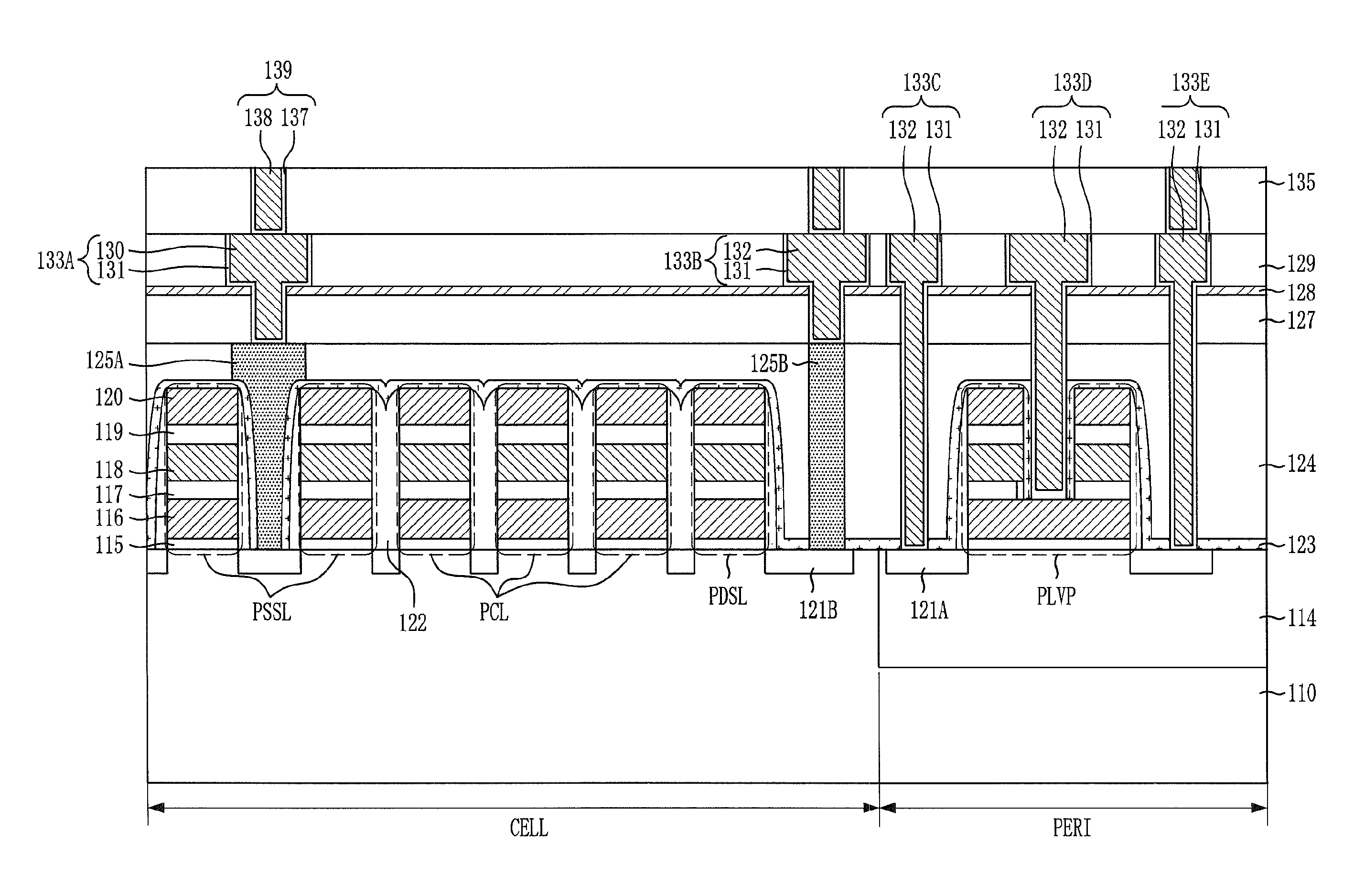
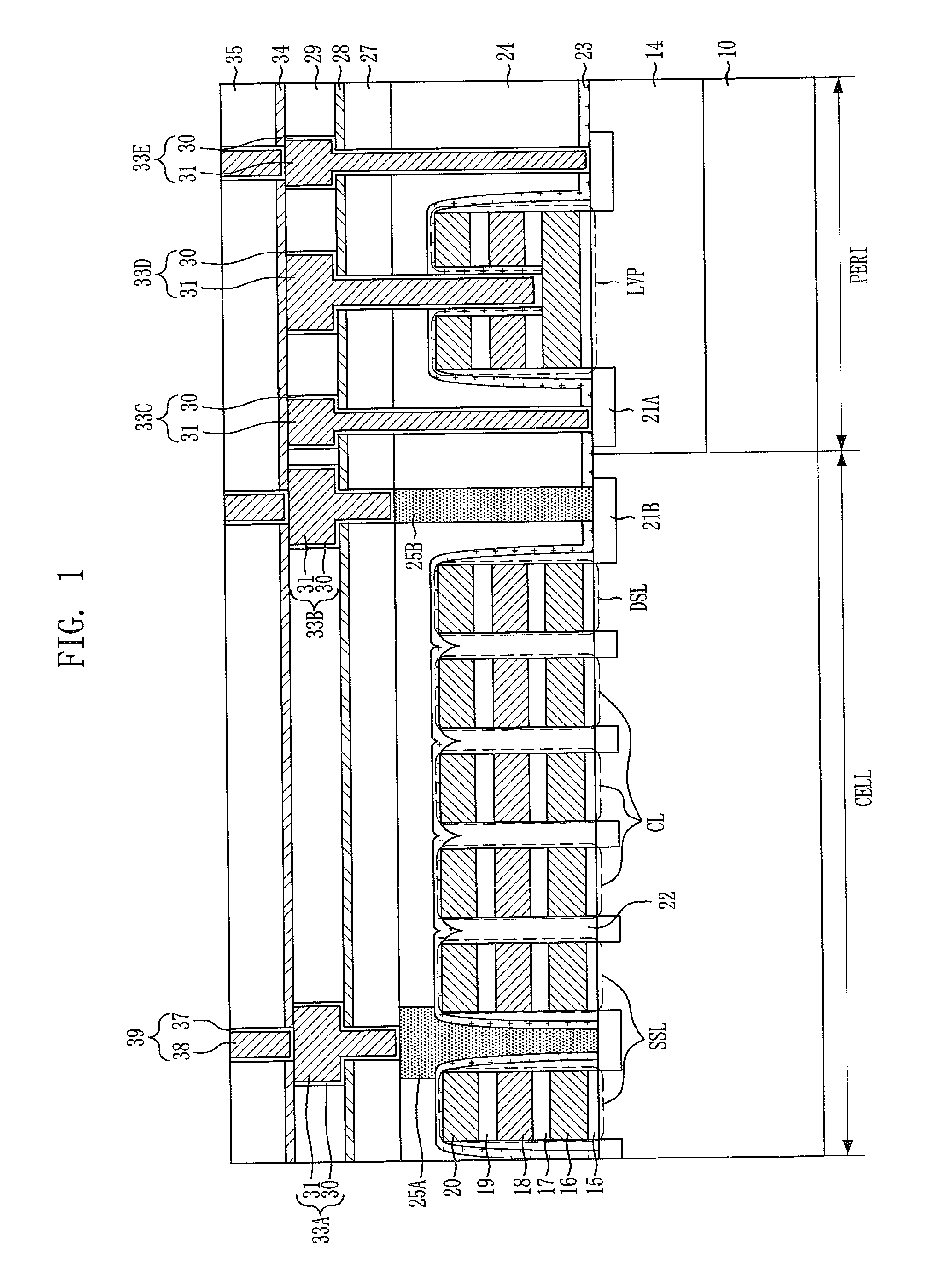
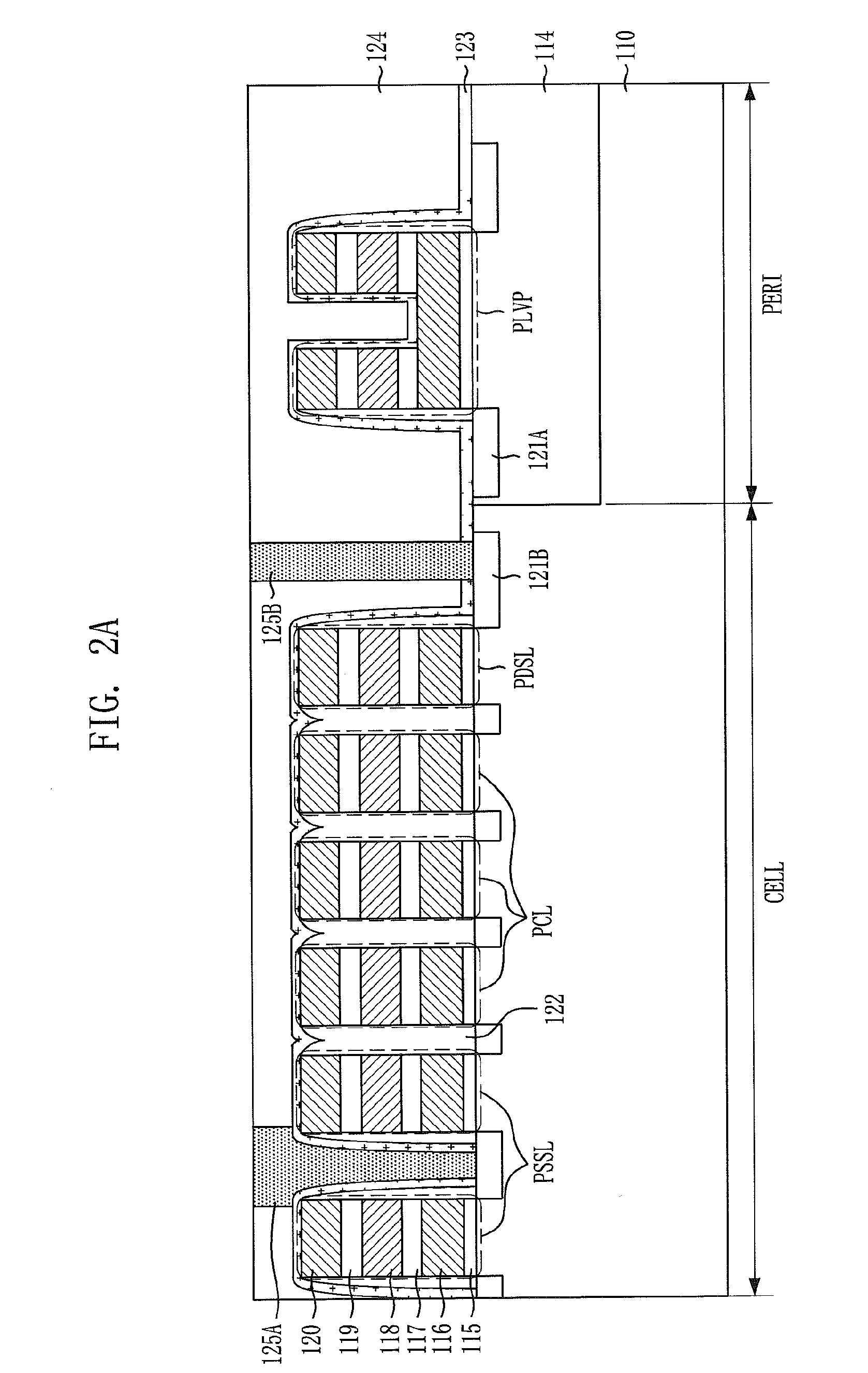
[0023]Referring to FIG. 2A, a substrate 110 (e.g., P-type substrate), which includes a cell region CELL and a peripheral region PERI, is provided. A triple N-type well, a deep P-type well and a shallow P-type well are formed in the cell region CELL, and an N-type well 114 is formed in the peripheral region PERI. A plurality of gate patterns for transistors are formed over the substrate 110. For example, first gate patterns PSSL for first transistors used to select one junction region (e.g. source region), second gate patterns PCS for memory cells and a third gate pattern PDSL for a second transistor used to select another junction region (e.g., drain region) are formed over the cell region CELL. A fourth gate pattern PLVP for a low voltage transistor is formed in the peripheral region PERI. Each of the first to fourth gate patterns PSSL, PCL, PDSL, and PLVP includes a structure laminated with a tunnel oxide layer 115, a floating gate 116, a dielectric layer 117, a control gate 118, ...


PUM


Abstract

A method for fabricating a semiconductor device includes forming a plurality of memory cells and transistors over a substrate, forming a first stopping layer having tensile stress over the plurality of memory cells and transistors, forming a first insulation layer over the substrate and the first stopping layer, and forming a second stopping layer having compression stress over the first insulation layer.

Description

CROSS-REFERENCE TO RELATED APPLICATIONS[0001]The present invention claims priority of Korean patent application number 2006-0095060, filed on Sep. 28, 2006 which is incorporated by reference in its entirety.BACKGROUND OF THE INVENTION[0002]The present invention relates to a method for fabricating a semiconductor memory device, and more particularly, to a method for fabricating a non-volatile memory device including a NAND flash memory device.[0003]A semiconductor memory is usually classified into a volatile memory, where stored information is erased upon stoppage of power supply, and a non-volatile memory, where stored information is retained despite of the stoppage of power supply. The non-volatile memory includes an erasable programmable read only memory (EPROM), an electrically EPROM (EEPROM), and a flash memory.[0004]The flash memory is distinguished into a NOR type and a NAND type according to the cell configuration. A cell array of a NAND memory includes a plurality of strings...

Claims


Application Information

Patent Timeline
Patent Type & Authority Applications(United States)
IPC IPC(8): H01L21/4763H01L21/469
CPCH01L21/3185H01L21/76807H01L27/11529H01L27/115H01L27/11526H01L21/76829H01L21/0217H01L21/02274H10B69/00H10B41/40H10B41/41H01L21/02107
Inventor CHOI, SE-KYOUNG
Owner SK HYNIX INC
Why Eureka
Try Eureka