Method of making iron silicide and method of making photoelectric transducer

a technology of iron silicide and photoelectric transducer, which is applied in the direction of coatings, chemical vapor deposition coatings, semiconductor devices, etc., can solve the problems of increasing process restrictions, adversely affecting the nature and characteristics of layers (films) and device characteristics, and increasing material costs, so as to eliminate bonding defects, influence on stability and film quality, and eliminate bonding defects in iron silicide films

Inactive Publication Date: 2006-01-05
TDK CORPARATION +1
View PDF16 Cites 12 Cited by
  • Summary
  • Abstract
  • Description
  • Claims
  • Application Information

AI Technical Summary

Benefits of technology

[0011] If such high temperature treatment is carried out when making a photoelectric transducer using β-FeSi2 in a semiconductor layer, for example, the amount of heat inputted to the substrate to be formed with a device may increase so as to change the form thereof. Using a highly heat resistant substrate for preventing such a problem from occurring increases the material cost, and the thermal budget of other layers (other semiconductor layers, electrode layers, protective layers, functional layers, etc.) constituting the device, which may adversely affect natures and characteristics of layers (films) and device characteristics while increasing restrictions on the process.
[0016] In view of such circumstances, it is an object of the present invention to provide a method and apparatus for making an iron silicide film, which can easily make an iron silicide film having a favorable film quality while being adapted to exhibit semiconductor characteristics and employable in a device having a large area. It is another object of the present invention to provide a method and apparatus for making a photoelectric transducer having excellent device characteristics by comprising such an iron silicide film, and a method and apparatus for making a photoelectric transducer unit comprising this device.
[0022] Preferably, in the pressure adjusting step, the fixed pressure is adjusted such that the iron silicide film attains a semiconductor characteristic. While the pressure about the substrate has a correlation with the concentration of chemical species such as active species, the possibility of colliding with neutral gases within a plasma space may rise disadvantageously depending on the ambient pressure and other film-forming conditions, whereby a sufficient amount of chemical species (reactive substances) may not reach the substrate surface. In particular, iron atoms have a greater mass than that of chemical species derived from the silicon-containing gas and hydrogen gas and thus seem to be more likely to be inhibited from migrating, whereby iron atoms are considered to be relatively hard to reach the substrate among various chemical species. For preventing this from happening, control for regulating the pressure about the substrate becomes effective.
[0025] While the iron silicide film formed by the making method of the present invention includes a hydrogen atom which can eliminate bonding defects, hydrogen may be desorbed from within the film depending on the temperature condition of the film. Also, details of whether dangling bonds are terminated with the equivalent amount of bonding defects or not are unclear. The possibility of hydrogen being physically occluded in the film cannot be denied. Further, the temperature of the substrate is assumed to be greatly influential on the stability and film quality (i.e., the amount of generated bonding defects) of the iron silicide structure. Therefore, for sufficiently eliminating the bonding defects in the iron silicide film, control for regulating the temperature of the substrate is effective.
[0029] More specifically, in the gas and iron supplying steps, it is preferred that the ratio between the flow rate of supply of the silicon-atom-containing gas and the amount of supply of the iron atom be adjusted such that the ratio (x:y) between the iron and silicon atoms in the iron silicide (FexSiy) film falls within the range of 1:1.7 to 1:3.5. This makes it easier for the iron silicide film to exhibit a semiconductor characteristic.

Problems solved by technology

Using a highly heat resistant substrate for preventing such a problem from occurring increases the material cost, and the thermal budget of other layers (other semiconductor layers, electrode layers, protective layers, functional layers, etc.) constituting the device, which may adversely affect natures and characteristics of layers (films) and device characteristics while increasing restrictions on the process.
However, such a resin film deforms plastically in an environment at several hundred degrees, and thus is very hard to employ the SPE, PDE, and MOCVD which require high-temperature treatment of 500° C. or higher in the forming process as mentioned above.

Method used


Image

  • Method of making iron silicide and method of making photoelectric transducer
  • Method of making iron silicide and method of making photoelectric transducer
  • Method of making iron silicide and method of making photoelectric transducer

Examples


example 1

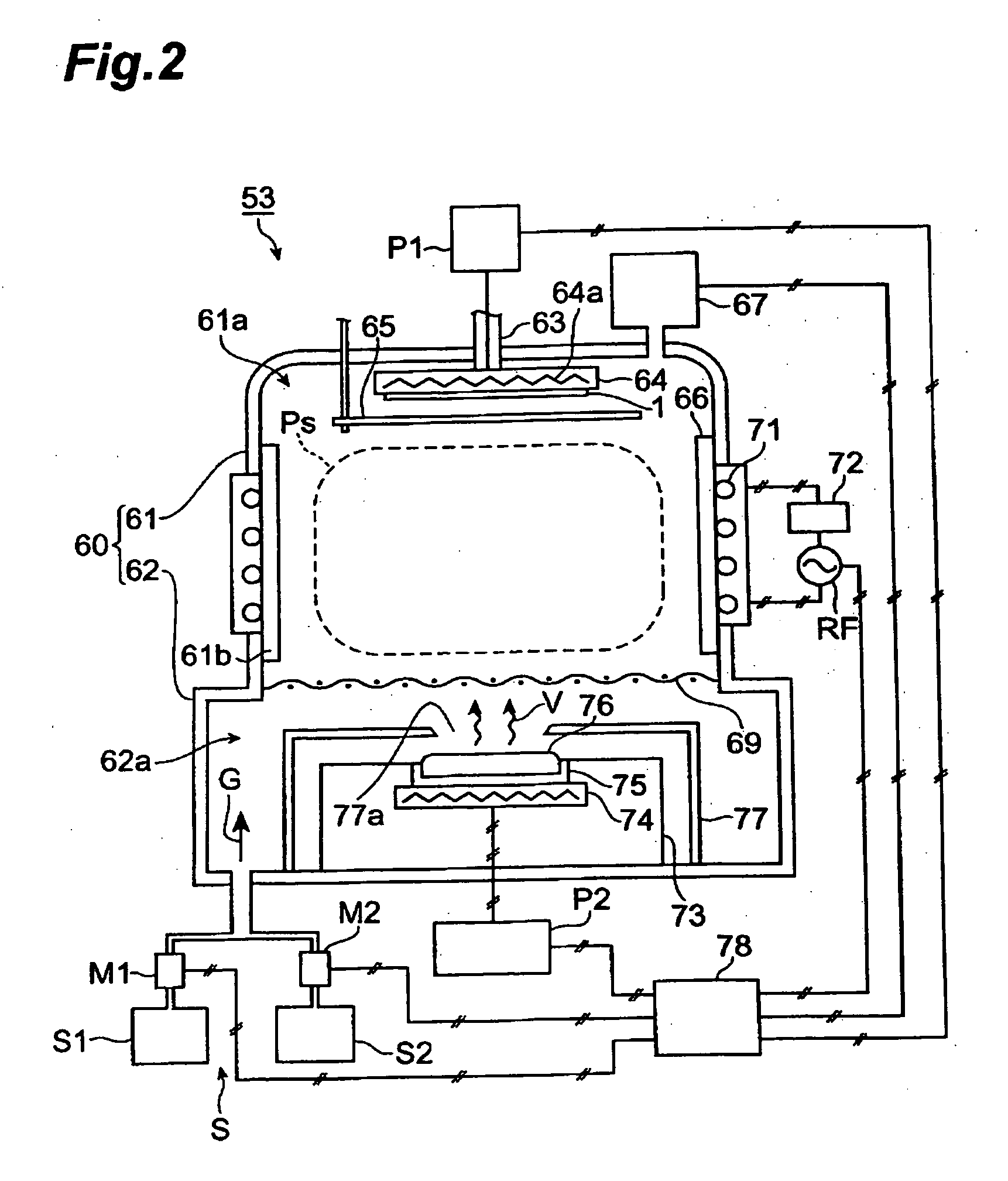
[0089] As a substrate, an Si wafer having a main surface with a surface orientation of (100) was accommodated in the upper part within a chamber, so as to be secured to a support table in a facedown fashion. The chamber was evacuated from the upper side of the chamber (the upper wall of the chamber opposing the rear side of the Si wafer) such that the pressure within the chamber became 1.33 Pa. While maintaining this pressure, a monosilane (SiH4) gas and a hydrogen (H2) gas each at a flow rate of 50 sccm were supplied into the chamber, and a high-frequency power of 50 W was applied to an L-coupling copper coil disposed about the chamber, so as to form a plasma of a mixed gas constituted by the monosilane gas and hydrogen gas.

[0090] Simultaneously with the forming of plasma, an iron ingot placed below the Si wafer was heated to about 1900° C. by resistance heating, and the iron vapor generated upon evaporation of iron was supplied into the plasma along the exhaust flow within the ch...

example 2

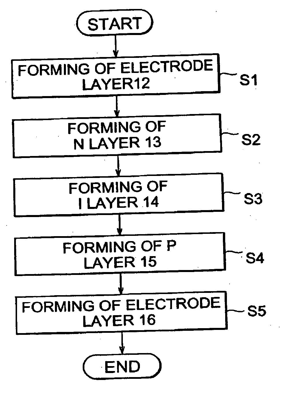
[0096] First, a metal electrode layer 12 having a thickness of 0.3 μm made of Ti was formed by sputtering on a glass substrate (substrate 11) having a main surface with a surface orientation of (100). Subsequently, an n layer 13 having a thickness of 30 nm made of n-type silicon was formed by plasma CVD on the metal electrode layer 12, and an i layer 14 made of an iron silicide film having a thickness of 400 nm was formed on the n layer 13 as in Example 1. Next, a p layer made of p-type silicon having a thickness of 20 nm was formed by plasma CVD on the i layer 14, so as to construct a p-i-n junction 100. Further, a transparent electrode layer 16 made of ITO having a thickness of 80 nm was formed on the p-i-n junction 100, so as to make a photoelectric transducer unit in accordance with the present invention configured as with the solar cell 10 shown in FIG. 3.

example 3

[0097] A photoelectric transducer unit in accordance with the present invention configured as with the hybrid solar cell 20 shown in FIG. 4 was made in the same manner as with Example 2 except that, after the i layer 14 (corresponding to the i layer 241) was formed, an i layer 242 made of amorphous silicon having a thickness of 200 nm was formed thereon by plasma CVD (under the film-forming condition with SiH4 flow rate of 20 sccm, H2 flow rate of 200 sccm, in-chamber pressure of 133 Pa, high-frequency power of 60 W, and substrate temperature of 200° C.), and that a p layer 15 was formed on the i layer 242, so as to construct a p-i-n junction 200.


PUM

PropertyMeasurementUnit
temperatureaaaaaaaaaa

Abstract

A solar cell comprises a substrate, and a metal electrode layer, a p-i-n junction, and a transparent electrode layer which are successively laminated on the substrate. The p-i-n junction comprises an n layer, an i layer, and a p layer which are laminated in this order. The i layer is made of an amorphous iron silicide film containing hydrogen in accordance with the present invention, and is formed on the n layer by supplying an iron vapor into a plasma of a material gas in which a silane type gas and a hydrogen gas are mixed. In the i layer, dangling bonds of silicon atoms and / or iron atoms are terminated with hydrogen, whereby a number of trap levels which may occur in the amorphous iron silicide film are eliminated.

Description

BACKGROUND OF THE INVENTION [0001] 1. Field of the Invention [0002] The present invention relates to a method and apparatus for making an iron silicide film, a method and apparatus for making an photoelectric transducer, and a method and apparatus for making a photoelectric transducer unit. [0003] 2. Related Background Art [0004] In recent years, compound semiconductors have widely been used in various optical devices, electronic devices, other devices, and the like. Among them, silicide semiconductors have been developed vigorously as materials which can exhibit excellent electric, optical, magnetic, and thermoelectric characteristics due to their complicated and diversified combining modes. Examples of silicide semiconductors include transitional metal silicide semiconductors typified by iron silicide, and alkaline earth silicide semiconductors typified by calcium silicide and magnesium silicide. In particular, attention has been focused on iron silicide as a material which is qui...

Claims


Application Information

Patent Timeline
Patent Type & Authority Applications(United States)
IPC IPC(8): H01L21/44C23C16/42C23C16/505H01L31/04H01L21/285
CPCC23C16/42Y02E10/548H01L21/28556C23C16/505
Inventor MOROOKA, HISAOYAMADA, HIROSHINISHI, KAZUO
Owner TDK CORPARATION
Why Eureka
Try Eureka