Process for producing photoelectric conversion devices

Active Publication Date: 2011-08-04
FUJIFILM CORP
View PDF1 Cites 11 Cited by
  • Summary
  • Abstract
  • Description
  • Claims
  • Application Information

AI Technical Summary

Benefits of technology

[0053]As described above, the inventors have found the film forming method, wherein a high-quality transparent conductive layer that appropriately covers the underlayer is formed with the electrolytic deposition technique such that a metal layer affecting a band gap structure within the photoelectric conversion device need not be formed. The utilization of the thus found film forming method has first enabled the process for producing a photoelectric conversion device, where

Problems solved by technology

In cases where the buffer layer is formed with the liquid phase technique, and the film formation of the transparent conductive layer, the window layer, and the like, which are formed at stages after the formation of the buffer layer, is performed by use of vacuum processing, such as a sputtering technique, it is not possible to perform continuous film formation, such as roll-to-roll mode film formation, and therefore complicated processing is required.
However, it is not always possible to form, with the liquid phase technique, the zinc oxide type of the transparent conductive layer which has good quality and which has a low electrical resistance value.
Accordingly, in the cases of the photoelectric

Method used


Image

  • Process for producing photoelectric conversion devices
  • Process for producing photoelectric conversion devices
  • Process for producing photoelectric conversion devices

Examples


examples

[0173]The present invention will further be illustrated by the following non-limitative examples.

examples 1 to 4

, Comparative Examples 1 to 3

[0174]In Examples 1 to 4 and Comparative Examples 1 to 3, photoelectric conversion devices were prepared by combining the layered substrates and the film forming techniques for the respective layers as described below. Table 1 shows the layer constitution, the combination of the film forming techniques for the respective layers, and the evaluation results in each of Examples 1 to 4 and Comparative Examples 1 to 3.

[0175]As the layered substrates, a layered substrate 1 and a layered substrate 2 described below were prepared.

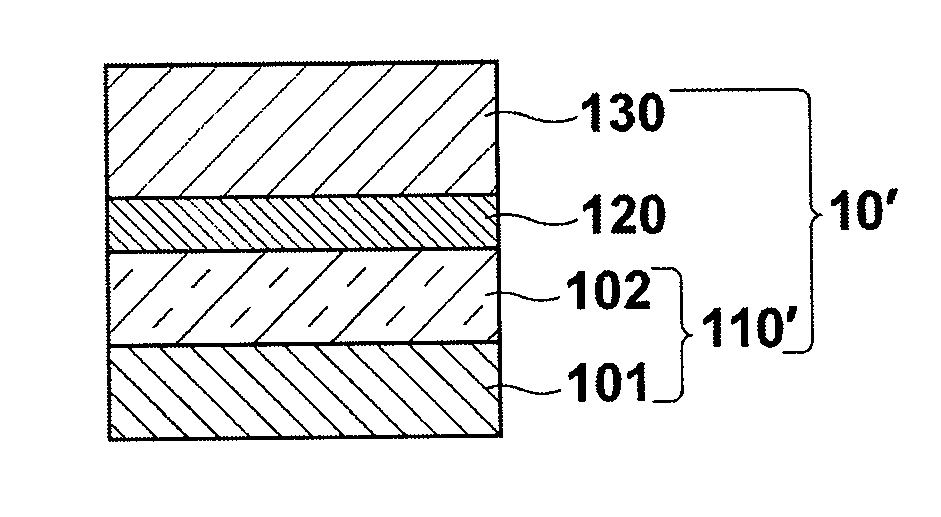
[0176]Layered substrate 1: The layered substrate 1 comprised a soda-lime glass (SLG) substrate provided with an Mo electrode layer, and a CIGS layer formed on the Mo electrode layer of the soda-lime glass (SLG) substrate. The layered substrate 1 was prepared in the manner described below.

[0177]The Mo bottom electrode layer having a thickness of 0.8 μm was formed with the sputtering technique on the soda-lime glass (SLG) substrate. A mas...


PUM


Abstract

In a process for producing a photoelectric conversion device comprising a bottom electrode layer, a photoelectric conversion semiconductor layer, a buffer layer, and a transparent conductive layer, which are stacked in this order on a substrate, all film forming stages ranging from a stage of forming the buffer layer to a stage of forming the transparent conductive layer are performed with a liquid phase technique. The buffer layer is formed with a chemical bath deposition technique, and the transparent conductive layer is formed with an electrolytic deposition technique.

Description

BACKGROUND OF THE INVENTION[0001]1. Field of the Invention[0002]This invention relates to a process for producing a photoelectric conversion device, such as a solar cell.[0003]2. Description of the Related Art[0004]Photoelectric conversion devices comprising a photoelectric conversion layer and electrodes electrically connected to the photoelectric conversion layer have heretofore been used in use applications, such as solar cells. Heretofore, as the solar cells, Si type solar cells utilizing bulk single crystalline Si or polycrystalline Si, or thin film amorphous Si have been most popular. Recently, research and development have been conducted on compound semiconductor type solar cells that do not depend upon Si. As the compound semiconductor type solar cells, there have been known bulk types, such as GaAs types, and thin film types, such as CIS or CIGS types which are constituted of a Group-Ib element, a Group-IIIb element, and a Group-VIb element. The CI (G) S types are the compo...

Claims


Application Information

Patent Timeline
IPC IPC(8): H01L31/18
CPCY02E10/541H01L31/18H01L31/1884H01L31/0749H01L31/03928H01L31/04
Inventor KAWANO, TETSUOKOIKE, TAKASHIAGUI, RYOUKO
Owner FUJIFILM CORP
Why Eureka
Try Eureka