Photoelectric converter, photoelectric conversion device and iron silicide film

a technology of photoelectric converter and conversion device, which is applied in the direction of photovoltaics, electrical devices, semiconductor devices, etc., can solve the problems of increasing the heat fed into the substrate to be formed with the device, changing shape, and affecting the degeneration and characteristics of the layer (film) and the device characteristics, so as to achieve excellent semiconductor characteristics, high conversion efficiency, and easy manufacturing

Inactive Publication Date: 2006-03-09
TDK CORPARATION +1
View PDF5 Cites 11 Cited by
  • Summary
  • Abstract
  • Description
  • Claims
  • Application Information

AI Technical Summary

Benefits of technology

[0010] For forming β-FeSi2 having a semiconductor characteristic, as can be seen from the descriptions of the above-mentioned prior publications, it is necessary for β-phase crystals to be grown sufficiently by high-temperature treatment at about 400 to 800° C. during or after performing its film-forming process. When the above-mentioned high-temperature treatment is performed at the time of manufacturing a photoelectric transducer or the like using β-FeSi2 as its i-layer, the amount of heat fed into a substrate to be formed with the device may increase, thereby causing changes in shape. If a highly heat-resistant substrate is used in order to suppress the changes in shape, the thermal budget with respect to layers (p-layers, n-layers, electrode layers, functional layers, etc.) other than the i-layer constituting the device will increase, thereby causing a fear of adversely affecting the degeneration and characteristics of layers (films) and device characteristics, while enhancing restrictions on the process. The use of the highly heat-resistant substrate increases the material cost as well.
[0014] In view of such circumstances, it is an object of the present invention to provide an iron silicide film which can easily be formed by low-temperature treatment (process) and can fully exhibit semiconductor characteristics, a photoelectric transducer having excellent device characteristics, and a photoelectric transducer apparatus equipped with the transducer.
[0022] Preferably, the above-mentioned first pin junction part further comprises a second i-layer disposed between the first p-layer and first n-layer and constituted by a mainly amorphous silicon film. Thus configured photoelectric transducer is a so-called hybrid device, i.e., one in which the intrinsic semiconductor layer in the first pin junction part is constituted by a composite layer including a first i-layer made of hydrogen-containing iron silicide (FexSiy:H) and a second i-layer made of amorphous silicon and / or microcrystalline silicon. The second i-layer exhibits a higher absorption coefficient for high-energy photons (short-wavelength photons) than does the first i-layer, so that the transducer as a whole can expand the absorption wavelength region, thereby increasing the output current.
[0026] The iron silicide film in accordance with the present invention, the photoelectric transducer using the same as an i-layer of a pin junction, and the photoelectric transducer apparatus equipped with the transducer can easily be manufactured by low-temperature treatment, so that adverse thermal influences on the substrate and the individual layers constituting the transducer can be eliminated, while excellent semiconductor characteristics can be exhibited, whereby a high conversion efficiency can be achieved, and device characteristics can be improved.

Problems solved by technology

When the above-mentioned high-temperature treatment is performed at the time of manufacturing a photoelectric transducer or the like using β-FeSi2 as its i-layer, the amount of heat fed into a substrate to be formed with the device may increase, thereby causing changes in shape.
If a highly heat-resistant substrate is used in order to suppress the changes in shape, the thermal budget with respect to layers (p-layers, n-layers, electrode layers, functional layers, etc.) other than the i-layer constituting the device will increase, thereby causing a fear of adversely affecting the degeneration and characteristics of layers (films) and device characteristics, while enhancing restrictions on the process.
The use of the highly heat-resistant substrate increases the material cost as well.
However, such resin films must deform in terms of compositions in an environment at several hundred degrees, which makes it very hard for a photoelectric transducer using β-FeSi2 as its i-layer necessitating high-temperature treatment at 400° C. or higher in the forming process as mentioned above to be disposed on such a resin film.
When trying to form β-FeSi2 by heat treatment at 400° C. or lower by relaxing the temperature condition, silicide crystals do not grow sufficiently, thus causing a problem of generating iron silicide which is substantially amorphous or made of microcrystals.
According to the inventors' findings, such amorphous or microcrystalline iron silicide tends to include many bonding defects, whereby a number of trap levels at different energy levels exist because of modes of these bonding defects.

Method used


Image

  • Photoelectric converter, photoelectric conversion device and iron silicide film
  • Photoelectric converter, photoelectric conversion device and iron silicide film
  • Photoelectric converter, photoelectric conversion device and iron silicide film

Examples


first embodiment

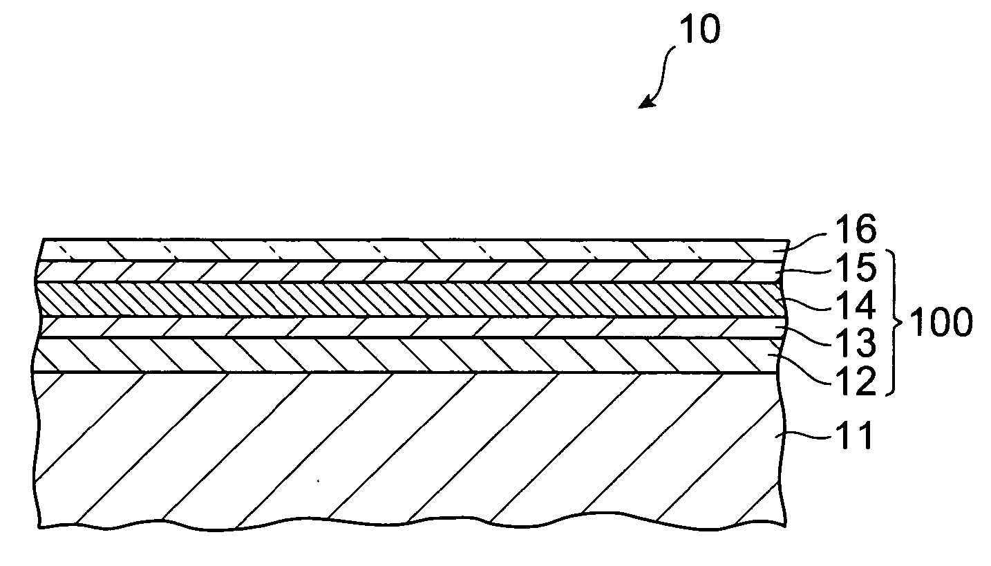
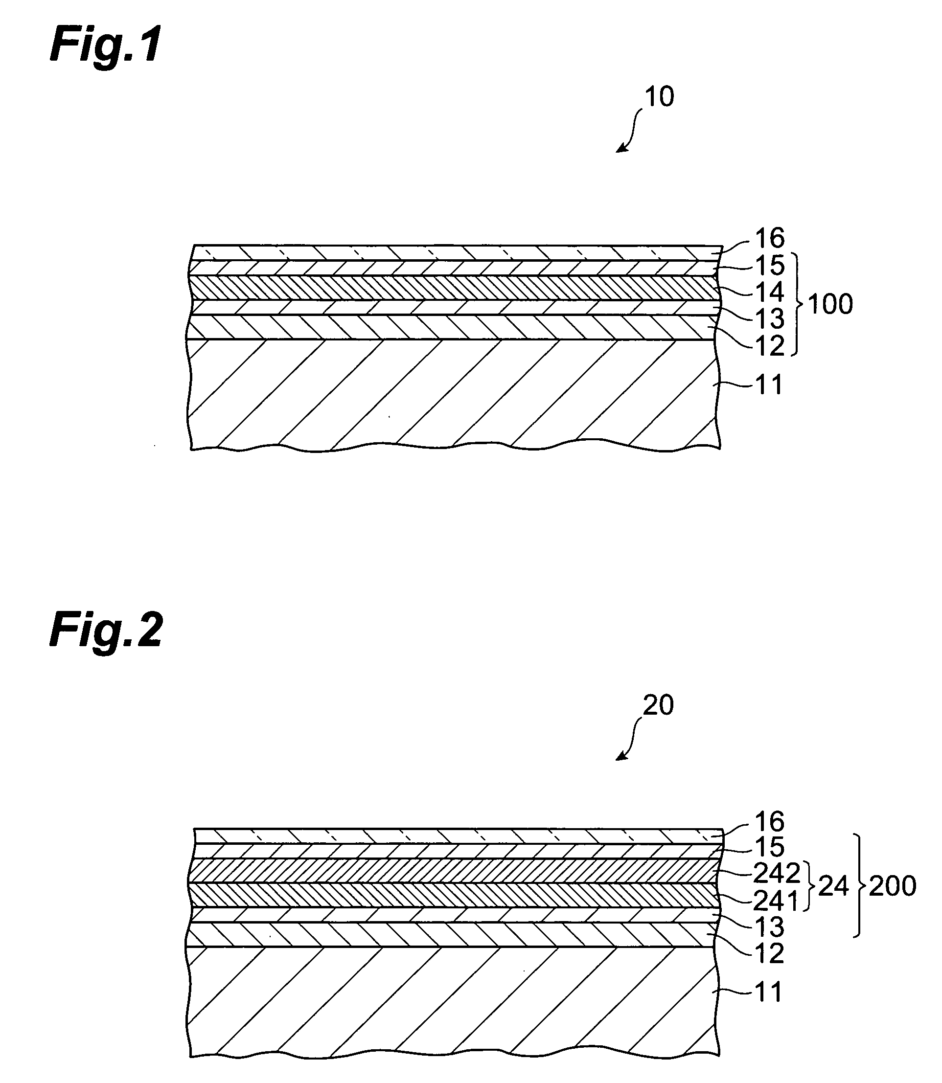
[0035]FIG. 1 is a schematic view showing a cross-sectional structure of the solar battery in accordance with a first embodiment. This solar battery 10 (photoelectric transducer) is one in which a metal electrode layer 12, a pin junction 100 (first pin junction part or photoelectric transducer), and a transparent electrode layer 16 are successively laminated on a substrate 11. Usable as the substrate 11 are silicon substrates, films made of polyamide resin or polyimide resin, etc.

[0036] Though not restricted in particular, the metal electrode layer 12 is preferably constituted by a material which exhibits a predetermined high conductivity and is hard to be damaged by a high-temperature atmosphere of about 400° C., while its reactivity with individual layers (which will be explained later) constituting the pin junction 100 is as low as possible. Preferred examples of such a material include rare metals such as Au, Pt, Pd, Ir, and Ag; rare metal alloys such as Au—Pd, Au—Pt, Ag—Pd, and...

second embodiment

[0049]FIG. 2 is a schematic view showing a cross-sectional structure of the solar battery in accordance with a second embodiment. This solar battery 20 (photoelectric transducer) has the same configuration as with the solar battery 10 shown in FIG. 1 except that it is equipped with a pin junction 200 (first pin junction part) in place of the pin junction 100. The pin junction 200 has the same configuration as with the pin junction 100 of the solar battery 10 except that it includes a composite i-layer 24 instead of the i-layer 14.

[0050] The composite i-layer 24 is constituted by an i-layer 241 (first i-layer or iron silicide film) made of amorphous FexSiy:H formed on the p-layer 13, and an i-layer 242 (second i-layer) made of amorphous silicon laminated on the first i-layer. Namely, the solar battery 20 is a hybrid photoelectric transducer apparatus in which a plurality of different kinds of i-layers are laminated. The i-layer 241 has the same structure as that of the i-layer 14 me...

third embodiment

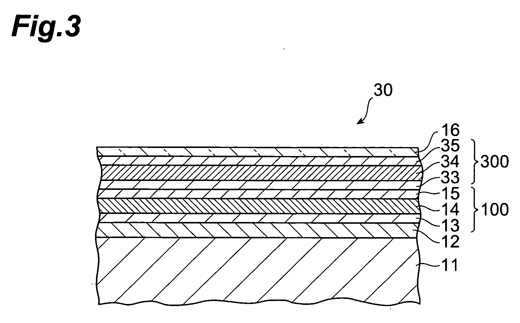
[0052]FIG. 3 is a schematic view showing a cross-sectional structure of the solar battery in accordance with a third embodiment. This solar battery 30 (photoelectric transducer apparatus) has the same configuration as with the solar battery 10 shown in FIG. 1 except that it further comprises a pin junction 300 (second pin junction part) between the pin junction 100 and the transparent electrode layer 16. The pin junction 300 comprises an n-layer 33 (second n-layer) formed like the n-layer 13, a p-layer 35 (second p-layer) formed like the p-layer 15, and an i-layer 34 (third i-layer) formed therebetween from amorphous silicon as with the i-layer 242.

[0053] Thus configured solar battery 30 is a tandem photoelectric transducer apparatus in which the pin junctions 100, 300 are arranged in series. Of photons incident on the i-layer 34 of the pin junction 300 by way of the transparent electrode layer 16, those having relatively short wavelengths are photoelectrically converted with a hig...


PUM

PropertyMeasurementUnit
temperatureaaaaaaaaaa
thicknessaaaaaaaaaa
thicknessaaaaaaaaaa

Abstract

A solar battery 10 comprises a metal electrode layer 12, a pin junction 100, and a transparent electrode layer 16 which are successively laminated on a substrate 11 such as a silicon substrate. The pin junction 100 comprises an n-layer 13, an i-layer 14, and a p-layer 15 which are laminated in succession. The i-layer 14 is formed by amorphous iron silicide (FexSiy:H) containing hydrogen atoms. In the i-layer 14, at least a part of the hydrogen atoms contained therein terminate dangling bonds of silicon atoms and / or iron atoms, so that a number of trap levels which may occur in an amorphous iron silicide film can be eliminated, whereby the i-layer 14 exhibits a characteristic as an intrinsic semiconductor layer.

Description

TECHNICAL FIELD [0001] The present invention relates to a photoelectric transducer, a photoelectric transducer apparatus, and an iron suicide film. BACKGROUND ART [0002] Materials such as group IV semiconductors (crystalline and amorphous types), compound semiconductors (group III-V, group II-VI, group I-III-VI, transition metal silicides, etc.), and organic semiconductors (coloring matters, polymers, etc.) have been in use in photoelectric transducers employed in solar batteries (cells) and the like. Among these device materials, the compound semiconductors are advantageous in that they have a high optical absorption coefficient and a bandgap (bandgap energy: Eg) suitable for yielding a favorable photoelectric conversion efficiency. [0003] Various structures such as pn junction, pin junction, and heterojunction have been known as modes of junctions of layers constituting a photoelectric transducer. The pin junction, in which a major part of photoelectrons and positive holes occur i...

Claims


Application Information

Patent Timeline
Patent Type & Authority Applications(United States)
IPC IPC(8): H01L31/105H01L31/06H01L31/00H01L31/04H01L31/0256H01L31/075H01L31/076
CPCH01L31/0264Y02E10/548H01L31/076H01L31/075
Inventor YAMADA, HIROSHIMOROOKA, HISAONISHI, KAZUO
Owner TDK CORPARATION
Why Eureka
Try Eureka