Active-matrix-driven display device

a display device and active matrix technology, applied in semiconductor devices, instruments, electrical apparatus, etc., can solve the problems of increased power consumption, increased power consumption, and the same problems are encountered in circuit configurations employing any other driving method

Inactive Publication Date: 2006-02-02
SANYO ELECTRIC CO LTD
View PDF1 Cites 294 Cited by
  • Summary
  • Abstract
  • Description
  • Claims
  • Application Information

AI Technical Summary

Benefits of technology

[0024] It is therefore an object of the present invention to provide an active-matrix-driven display device that operates with reduced variation of brightness attributable to time-related or temperature-related variation with no increase in power consumption.

Problems solved by technology

Disadvantageously, however, setting the operating points in that way is equivalent to making the differential voltage between the supply voltages VDD and CV greater, and thus leads to increased power consumption.
Moreover, to satisfactorily avoid the influence of time-related and temperature-related variation, the operating points need to be so set that they remain within the saturation region of the driving transistor TR103 even when, in the presence of time-related or temperature-related variation, the VOLED-IOLED characteristic shifts as indicated by the broken line 202 (specifically, the driving transistor TR103 needs to be operated in a higher-voltage part of the saturation region thereof), leading to increased power consumption.
It should be understood that, although the above discussion of the conventionally experienced problems assumes a circuit configuration employing a voltage program driving method, the same problems are encountered also in circuit configurations employing any other driving methods.

Method used


Image

  • Active-matrix-driven display device
  • Active-matrix-driven display device
  • Active-matrix-driven display device

Examples


first embodiment

[0159] A first embodiment of the present invention as applied to an organic EL display device will be specifically described below with reference to the relevant drawings.

FIG. 1—Overall Configuration Block Diagram

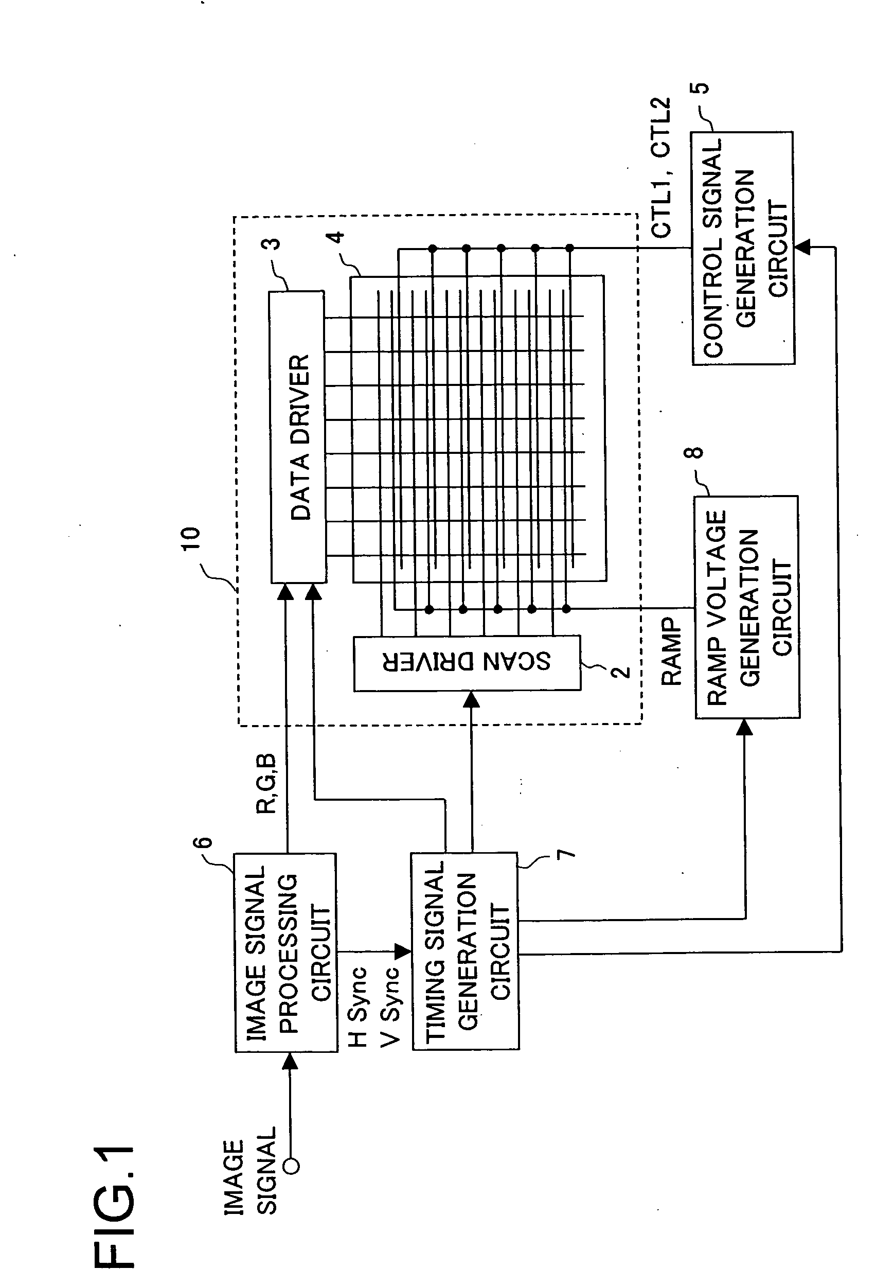
[0160]FIG. 1 is a block diagram showing the overall configuration of the organic EL display device of a first embodiment of the present invention. As shown in FIG. 1, the organic EL display 10 has a display panel 4 composed of a plurality of pixels arrayed in a matrix, and this display panel 4 is connected to: a scan driver 2 that feeds a scan voltage to each pixel; a data driver 3 that feeds a data voltage to each pixel; a ramp voltage generation circuit 8; and a control signal generation circuit 5. The organic EL display device shown in FIG. 1 displays on the display panel 4 an image according to an image signal fed from an image source (external signal source) such as a television receiver (unillustrated).

[0161] The image signal fed from an image source such as a tele...

second embodiment

[0195] A second embodiment of the present invention as applied to an organic EL display device will be described below. The overall configuration of the organic EL display device of the second embodiment of the present invention is substantially the same as that shown in FIG. 1; therefore, no separate diagram is furnished in that aspect, and the following description places emphasis on differences from the first embodiment.

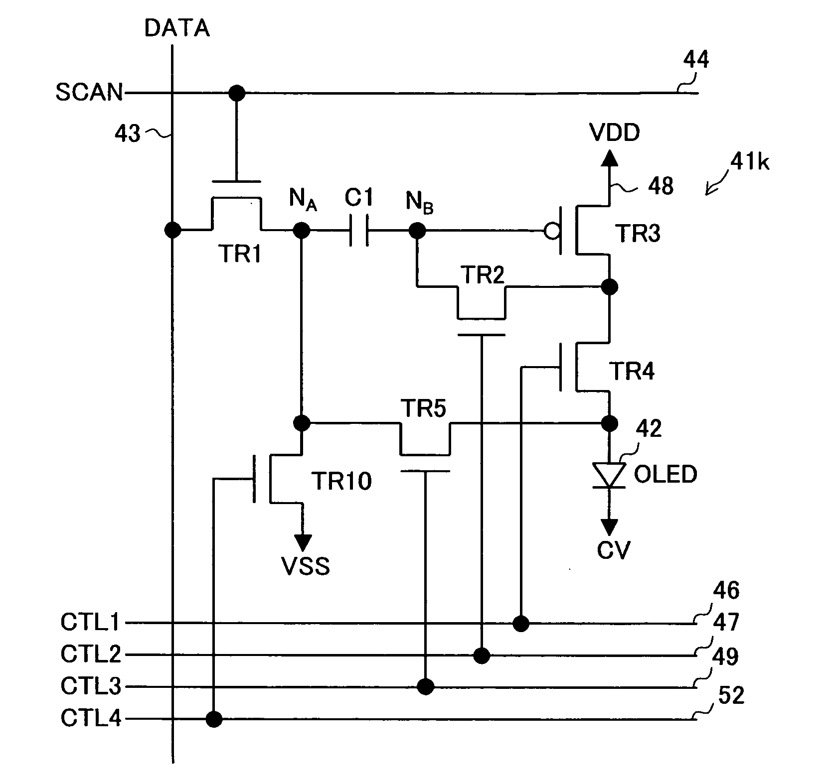
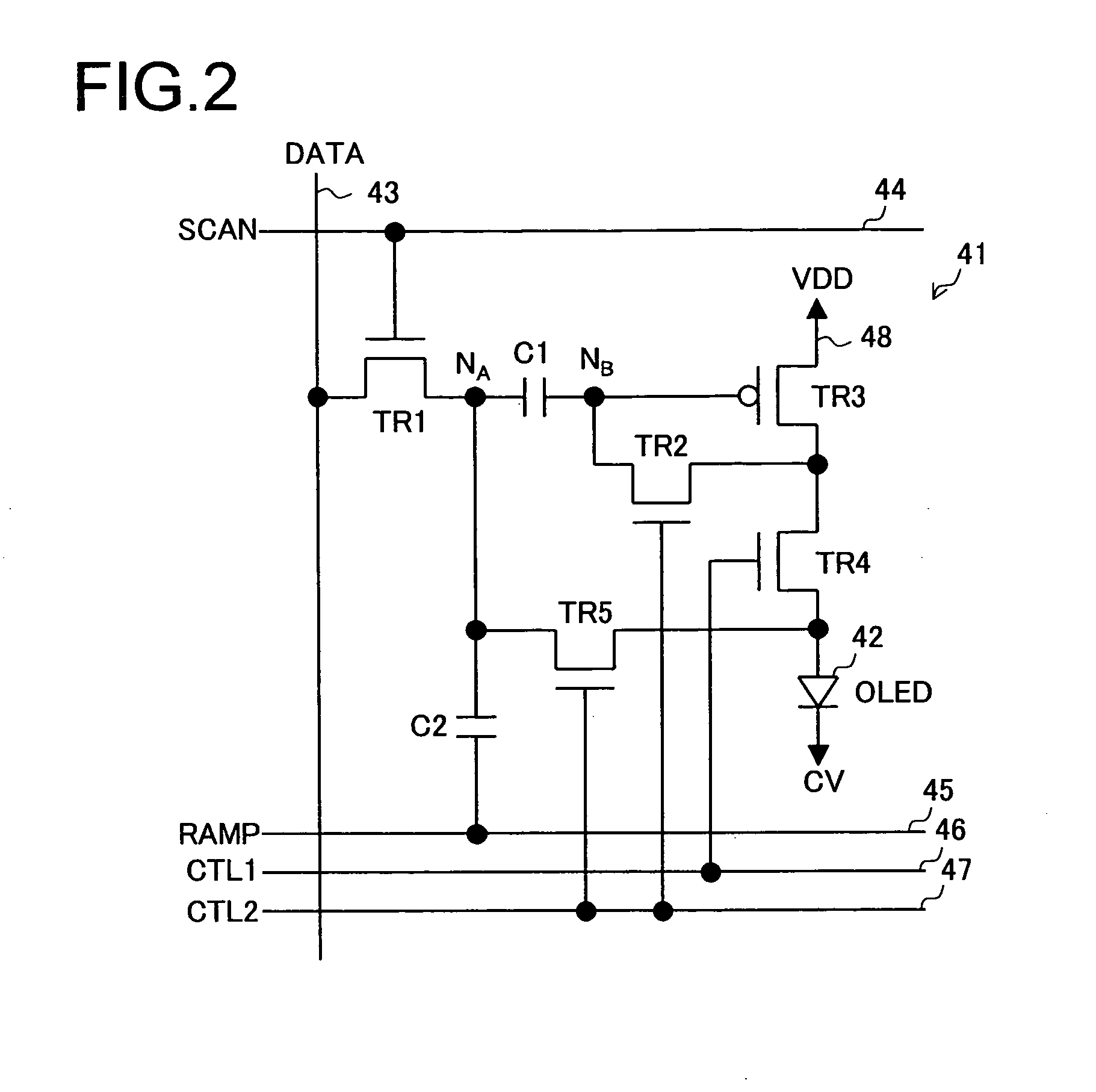
[0196] The display panel 4 is so modified that each pixel 41a constituting it is configured as shown in FIG. 5. In FIG. 5, such elements as are found also in FIG. 2 are identified with common reference numerals and symbols, and no overlapping explanations will be repeated. The pixel 41a (the pixel circuit of the pixel 41a) differs from the pixel 41 (the pixel circuit of the pixel 41) shown in FIG. 2 in the following respects: a resetting transistor TR6 is additionally provided of which the first electrode (for example, drain) and the second electrode (for example...

third embodiment

[0204] A third embodiment of the present invention as applied to an organic EL display device will be described below. The overall configuration of the organic EL display device of the third embodiment of the present invention is substantially the same as that shown in FIG. 1; therefore, no separate diagram is furnished in that aspect, and the following description places emphasis on differences from the first embodiment.

[0205] The display panel 4 is so modified that each pixel 41b constituting it is configured as shown in FIG. 7. In FIG. 7, such elements as are found also in FIG. 2 are identified with common reference numerals and symbols, and no overlapping explanations will be repeated. The pixel 41b (the pixel circuit of the pixel 41b) differs from the pixel 41 (the pixel circuit of the pixel 41) shown in FIG. 2 in the following respects: a PWM circuit (pulse width modulation circuit) 50 is provided between the second electrode of the writing transistor TR1 and the node NA; the...


PUM


Abstract

In a display panel, each pixel has a display element that emits light when fed with electric power, a writing transistor, a driving transistor that drives the display element, a first capacitive element that is provided in series with a line connecting the second electrode of the writing transistor and the control electrode of the driving transistor, and an adjustment transistor that, during a reset period, is turned on to feed a voltage commensurate with the electrode-to-electrode voltage of the display element to the writing-transistor-side electrode of the first capacitive element. A control signal generation circuit is provided that, during the reset period, lets a voltage commensurate with the light emission start electrode-to-electrode voltage of the display element be held in the first capacitive element.

Description

[0001] This application is based on Japanese Patent Application No. 2004-223765 filed on Jul. 30, 2004, Japanese Patent Application No. 2005-093490 filed on Mar. 29, 2005, and Japanese Patent Application No. 2005-176279 filed on Jun. 16, 2005, the contents of which are hereby incorporated by reference. BACKGROUND OF THE INVENTION [0002] 1. Field of the Invention [0003] The present invention relates to a display device in which a display element such as an organic electroluminescent (EL) element is driven by the use of switching devices such as thin-film transistors (TFTs), and more particularly to an active-matrix-driven display device. [0004] 2. Description of Related Art [0005] In recent years, many advancements have been made in the development of organic electroluminescent displays (hereinafter organic EL displays; likewise display devices employing organic EL displays will hereinafter be referred to as organic EL display devices), and studies have been made on the application o...

Claims


Application Information

Patent Timeline
Patent Type & Authority Applications(United States)
IPC IPC(8): H01L27/082
CPCG09G3/2014G09G3/3233G09G2300/0819G09G2300/0842G09G2300/0852G09G2320/045G09G2300/0876G09G2310/066G09G2320/0238G09G2320/0285G09G2320/043G09G2300/0861
Inventor YAMASHITA, ATSUHIRO
Owner SANYO ELECTRIC CO LTD
Why Eureka
Try Eureka