
Printed circuit substrate appearance inspection method, printed circuit substrate appearance inspection program and printed circuit substrate appearance inspection apparatus

a technology of printed circuit substrate and appearance inspection method, which is applied in the direction of image enhancement, image analysis, instruments, etc., can solve the problems of affecting the appearance inspection accuracy the position or the size of silkscreen printed parts may vary, etc., and achieve the effect of avoiding situations and reducing the accuracy of appearance inspection

Inactive Publication Date: 2006-02-02
FUJITSU LTD
View PDF7 Cites 6 Cited by
  • Summary
  • Abstract
  • Description
  • Claims
  • Application Information

AI Technical Summary

Benefits of technology

[0015] The present invention has been devised in consideration of the above-mentioned problem, and an object of the present invention is to provide a scheme by which, when appearance inspection is carried out on an electronic component mounted on a printed circuit substrate on which a printed circuit pattern part such as a silkscreen printed part is formed, it is possible to avoid degradation of inspection accuracy otherwise occurring due to the presence of the printed substrate pattern part as mentioned above.
[0017] In this scheme according to the present invention, since the inspection area is defined in such a manner that no printed substrate pattern part may be included in the inspection area, it is possible to effectively avoid a situation that the printed substrate pattern may degrade the appearance inspection accuracy.

Problems solved by technology

A position or a size of the silkscreen printed part may vary due to printing error or such.
However, when various sorts of inspections are carried out as a result of carrying out information processing on an image obtained from taking a photograph of a printed circuit substrate regarded as a to-be-inspected product during appearance inspection of the printed circuit substrate as mentioned above, the following problems may occur.

Method used


Image

  • Printed circuit substrate appearance inspection method, printed circuit substrate appearance inspection program and printed circuit substrate appearance inspection apparatus
  • Printed circuit substrate appearance inspection method, printed circuit substrate appearance inspection program and printed circuit substrate appearance inspection apparatus
  • Printed circuit substrate appearance inspection method, printed circuit substrate appearance inspection program and printed circuit substrate appearance inspection apparatus

Examples


Embodiment Construction

[0027] With reference to FIGS. 4 and 5, an embodiment of the present invention is described below.

[0028] According to the embodiment of the present invention, as one example of a printed substrate pattern part described below, a silkscreen printed part is applied.

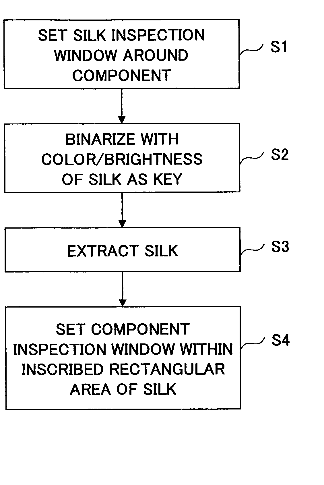
[0029]FIG. 4 is a flow chart showing a method of setting a component inspection window for carrying out appearance inspection on an electronic component mounted on a printed circuit substrate according to the embodiment of the present invention.

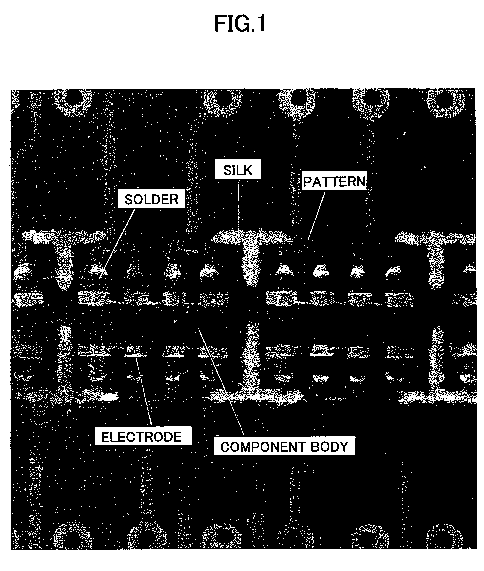
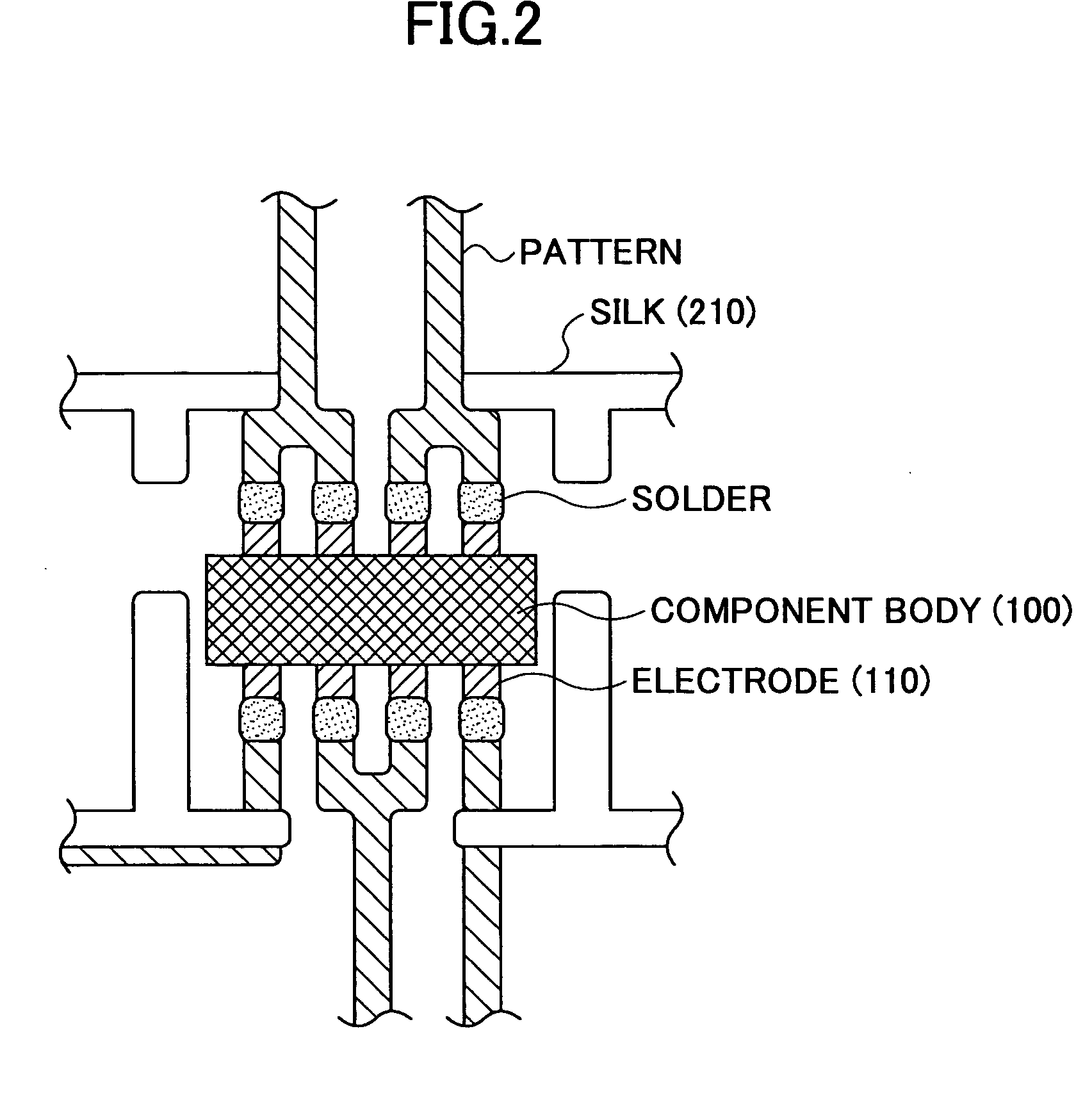
[0030] In Step S1, first, a silk inspection window is set around a relevant electronic component 100. This silk inspection window is set in such a manner as to define an area around the relevant electronic component 100, which is an area around electrodes 110 of the electronic component 100 and lands 200 on the printed circuit substrate to which lands the electrodes 110 are soldered. However, the area defined by the silk inspection window is defined in such a manner that it does n...


PUM


Abstract

A printed circuit substrate appearance inspection method comprising: an inspection area defining step defining a predetermined inspection area on an image of a printed circuit substrate including a component mounted on the printed circuit substrate; and an appearance inspection step carrying out appearance inspection of the component by analyzing image data in the thus-defined inspection area, wherein: the inspection area defining step comprises the steps of; detecting a printed substrate pattern part around the component on the printed circuit substrate; and defining the predetermined inspection without overlapping with the thus-detected printed substrate pattern part.

Description

BACKGROUND OF THE INVENTION [0001] 1. Field of the Invention [0002] The present invention relates to a printed circuit substrate appearance inspection method, a printed circuit substrate appearance inspection program and a printed circuit substrate appearance inspection apparatus, and, in particular, to a printed circuit substrate appearance inspection method, a printed circuit substrate appearance inspection program and a printed circuit substrate appearance inspection apparatus advantageous in particular for a printed circuit substrate having a printed substrate pattern part such as a silkscreen printed part. [0003] 2. Description of the Related Art [0004] Inspection of respective electronic components mounted on a printed circuit substrate carried out before shipping the circuit substrate which will be then used in an electronic apparatus or such, includes a verification as to whether or not predetermined electronic components are positively mounted, whether or not the mounted po...

Claims


Application Information

Patent Timeline
IPC IPC(8): G06K9/00
CPCG06T2207/30141G06T7/0004
Inventor WAKABAYASHI, AKIHIRO
Owner FUJITSU LTD
Learn More