Display device
- Summary
- Abstract
- Description
- Claims
- Application Information
AI Technical Summary
Benefits of technology
Problems solved by technology
Method used
Image

Examples
first embodiment
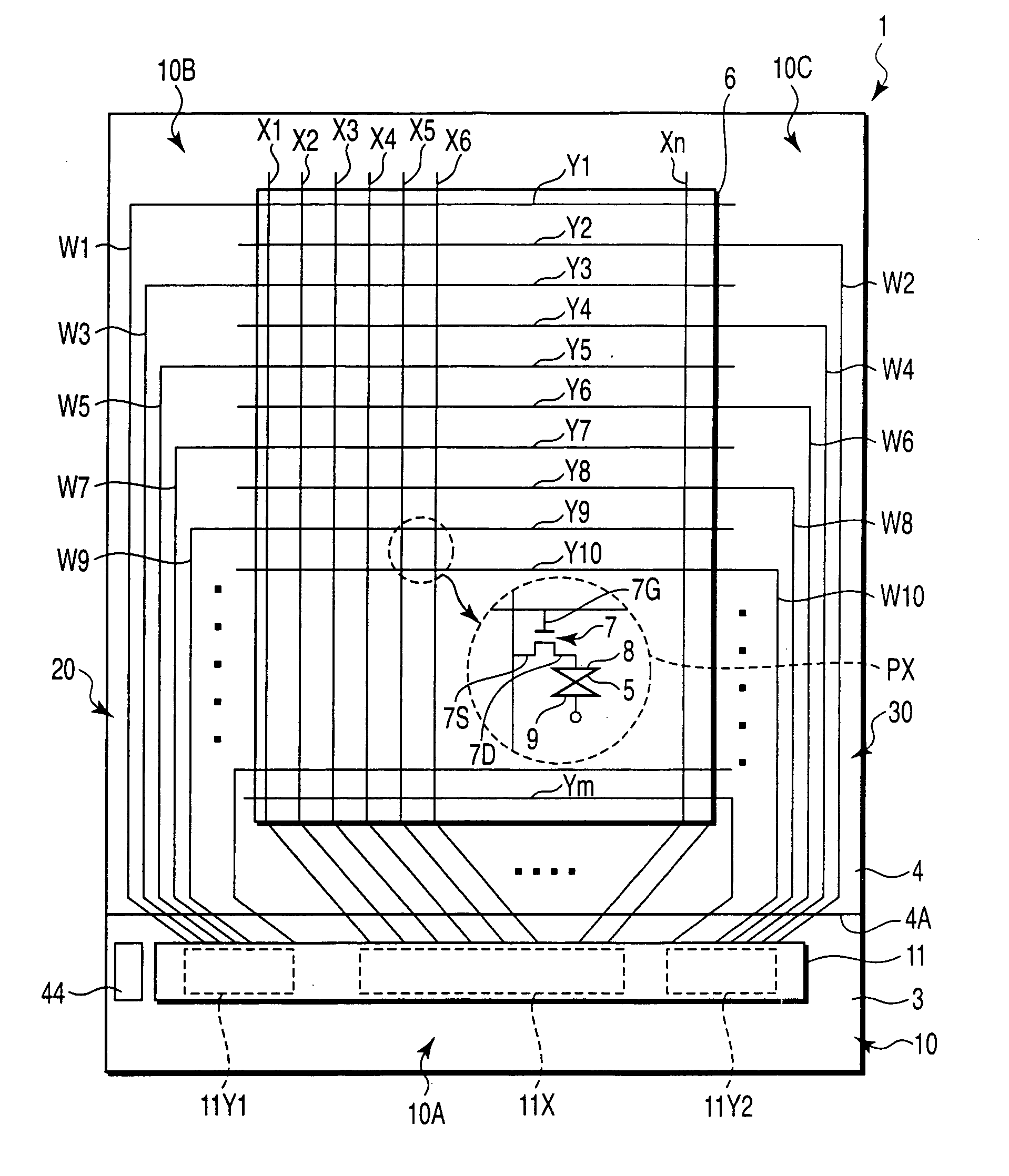
[0023] As is shown in FIG. 1, a liquid crystal display device, which is an example of a display device includes a substantially rectangular, planar liquid crystal display panel 1. The liquid crystal display panel 1 comprises a pair of substrates, that is, an array substrate 3 and a counter-substrate 4, and a liquid crystal layer 5 that is interposed as an optical modulation layer between the pair of substrates. The liquid crystal display panel 1 includes a rectangular effective display section 6 that displays an image. The effective display section 6 is composed of a plurality of display pixels PX that are arranged in a matrix.
[0024] The array substrate 3 includes, in the effective display section 6, a plurality of scan lines Y (1, 2, 3, . . . , m) that extend in a row direction of the display pixels PX, a plurality of signal lines X (1, 2, 3, . . . , n) that extend in a column direction of the display pixels PX, switching elements 7 that are arranged for the respective display pix...
second embodiment
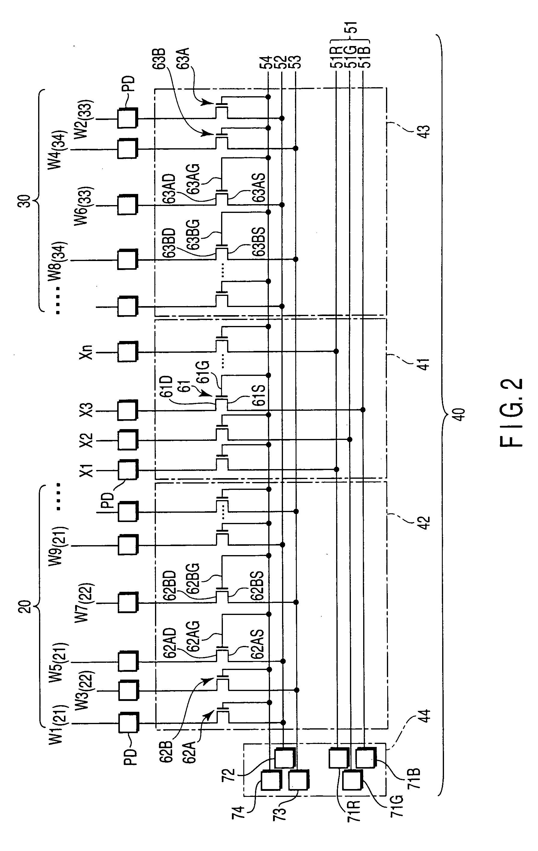
[0080] In the second embodiment, as shown in FIG. 5, the array substrate 3 includes an inspection wiring line section 40 for inspecting a wiring defect between the lines of the first wiring line group 20 and a wiring defect between the lines of the second wiring line group 30 on the peripheral part 10, and a wiring defect in the effective display section 6. The inspection wiring line section 40 includes a signal line inspection section 41 that is provided in association with the signal line driving section 11X, a first scan line inspection section 42 that is provided in association with the first driving unit 11Y1 of the scan line driving section 11Y, a second scan line inspection section 43 that is provided in association with the second driving unit 11Y2 of the scan line driving section 11Y, and a pad section 44 for inputting various signals to the respective inspection sections 41, 42 and 43.
[0081] The signal line inspection section 41 includes signal line inspection wiring lines...
PUM
 Abstract
Description
Claims
Application Information
 - R&D
- Intellectual Property
- Life Sciences
- Materials
- Tech Scout
- Unparalleled Data Quality
- Higher Quality Content
- 60% Fewer Hallucinations
Browse by: Latest US Patents, China's latest patents, Technical Efficacy Thesaurus, Application Domain, Technology Topic, Popular Technical Reports.
© 2025 PatSnap. All rights reserved.Legal|Privacy policy|Modern Slavery Act Transparency Statement|Sitemap|About US| Contact US: help@patsnap.com