Method for managing display memory data of light emitting display

a technology of light-emitting displays and memory data, which is applied in the direction of electroluminescent light sources, static indicating devices, instruments, etc., can solve the problems of reducing the aperture ratio of pixels and difficult to arrange these elements in a single pixel, so as to improve memory efficiency, reduce data access time, and read easily

Active Publication Date: 2006-02-23
SAMSUNG DISPLAY CO LTD
View PDF40 Cites 15 Cited by
  • Summary
  • Abstract
  • Description
  • Claims
  • Application Information

AI Technical Summary

Benefits of technology

[0013] In another exemplary embodiment according to the present invention, a light emitting display sorts display data into a form that can be read easily from the memory, and stores and manages the sorted display data, thereby reducing the data access time and enhancing the memory efficiency.

Problems solved by technology

Also, since many transistors, capacitors, and lines for transmitting voltages or signals are required for one pixel, it is difficult to arrange these elements in a single pixel.
Further, since data lines are respectively formed corresponding to the R, G, and B pixels at the limited display area and the drivers for driving theses pixels are respectively formed therein, there is a problem in which the aperture ratio of pixels is reduced.

Method used


Image

  • Method for managing display memory data of light emitting display
  • Method for managing display memory data of light emitting display
  • Method for managing display memory data of light emitting display

Examples


Embodiment Construction

[0030] In the following detailed description, only certain exemplary embodiments of the invention are shown and described, simply by way of illustration. As those skilled in the art would realize, the described embodiments may be modified in various different ways, all without departing from the spirit or scope of the invention. Accordingly, the drawings and description are to be regarded as illustrative in nature, and not restrictive. There may be parts shown in the drawings, or parts not shown in the drawings, that are not discussed in the specification as they are not essential to a complete understanding of the invention. Like reference numerals designate like elements.

[0031] Hereinafter, a managing method for managing display memory data of a light emission display according to an exemplary embodiment of the present invention will be described in detail with reference to the accompanying drawings.

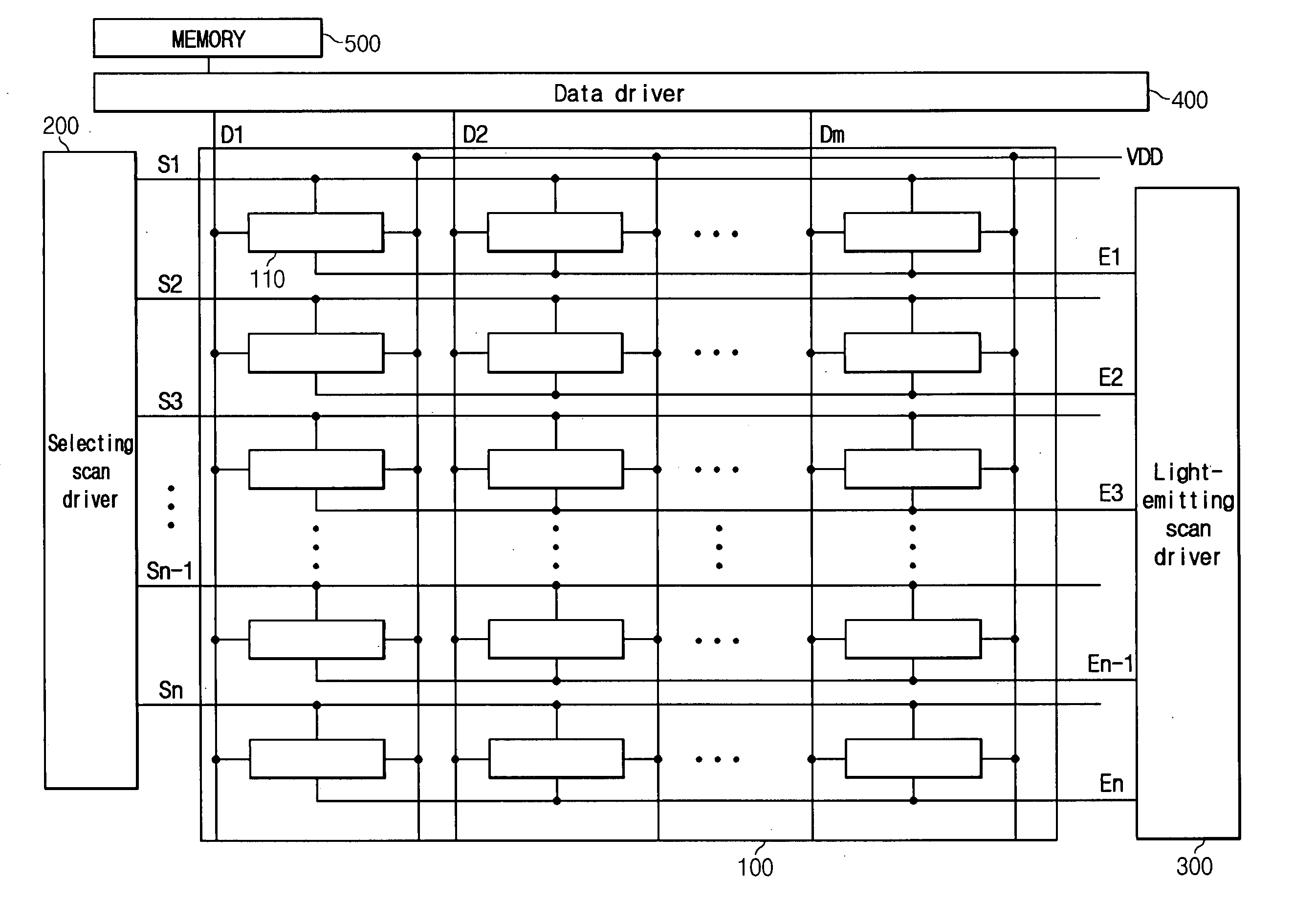
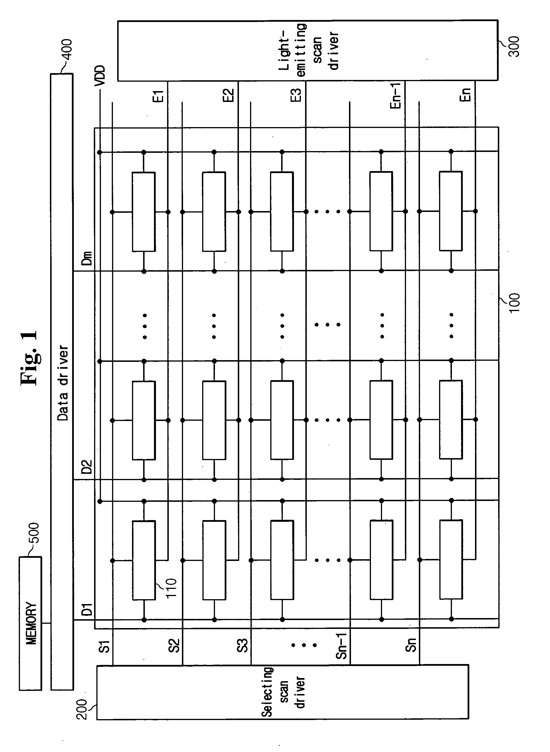
[0032]FIG. 1 is a schematic plain view of an organic light emitting display.

[00...


PUM


Abstract

A memory managing method for display data of a light emitting display device, which uses field light-emitting of organic materials. A plurality of pixels are each provided with at least two sub-pixels to emit different color lights, wherein one field has at least first and second subfields divided and driven independently. At least two data signals corresponding to substantially the same color are time-divided and applied to a data line during the one field, and selecting signals are sequentially applied to a plurality of scan lines at the first and second subfields. The method includes a) dividing input data corresponding to a display image into data for the first and second subfields, b) arranging the data for the first and second subfields according to a sequence of light-emitting driving, and c) storing the arranged data as pixel-based data.

Description

CROSS REFERENCE TO RELATED APPLICATION [0001] This application claims priority to and the benefit of Korean Patent Application No. 10-2004-0065778 filed on Aug. 20, 2004 in the Korean Intellectual Property Office, the entire content of which is incorporated herein by reference. BACKGROUND OF THE INVENTION [0002] 1. Field of the Invention [0003] The present invention relates to a method for managing display memory data of a light emitting display, and more particularly, it relates to a method for managing display memory data of an organic light emitting display (referred to as an “OLED” hereinafter) using light emission of organic materials. [0004] 2. Description of the Related Art [0005] Generally, an active matrix display such as a liquid crystal display and an OLED includes a plurality of scan lines arranged in the row direction and a plurality of data lines arranged in the column direction at the display area. Neighboring scan lines and data lines define each pixel area, and a pl...

Claims


Application Information

Patent Timeline
Patent Type & Authority Applications(United States)
IPC IPC(8): G09G3/30H05B44/00
CPCG09G3/2022G09G3/3233G09G5/399G09G2300/0452G09G2320/043G09G2300/0804G09G2300/0819G09G2300/0852G09G2300/0861G09G2300/0465G09G3/30G09G3/20G09G3/36
Inventor LEE, KYOUNG-SOOSONG, JUNE-YOUNG
Owner SAMSUNG DISPLAY CO LTD
Why Eureka
Try Eureka