
Manufacturing methods and electroless plating apparatus for manufacturing wiring circuit boards

a manufacturing method and electroless technology, applied in the direction of printed circuits, electrical devices, printed circuit manufacturing, etc., to achieve the effect of enhancing yield and reducing thickness fluctuations

Inactive Publication Date: 2006-03-02
NGK SPARK PLUG CO LTD
View PDF5 Cites 9 Cited by
  • Summary
  • Abstract
  • Description
  • Claims
  • Application Information

AI Technical Summary

Benefits of technology

[0008] In light of the foregoing problems, it is hence an object of the invention to provide a manufacturing method for a wiring circuit board which is capable of enhancing the yield and of unifying the electrical characteristics among the products, by reducing the fluctuations in thickness of electroless Cu plating film. It is another object to provide an electroless plating apparatus for executing this manufacturing method.
[0014] According to the invention, all wiring circuit board workpieces are contacted uniformly by the bubbles, and fresh electroless Cu plating liquid permeates into all parts, thereby decreasing variations or fluctuations of the thickness of the electroless Cu plating film. Moreover, because an electroless Cu plating film is well formed in the vias of the workpieces, the conduction characteristics and connection reliability of the vias are improved. As a result, the number of wiring circuit boards rejected during shipping inspections is decreased. Further, the method used promotes uniformity in the electrical characteristics among the products produced, i.e., from product to product.
[0018] In accordance with another aspect of the invention, a plurality of wiring circuit board workpieces are suspended at equal intervals on a rack. The rack is adapted to be immersed in the plating bath so that the spacing interval of the wiring circuit board workpiece and the bubble generator can be maintained constant. Hence, the distance or spacing between the bubble generator and wiring circuit board workpieces can be easily controlled, so as to ensure that the bubbles will uniformly contact with the wiring circuit board workpieces.
[0019] In preferred embodiments, the bubble generator includes bubble ejection holes arranged in rows so as to eject bubbles at an angle to the horizontal. Preferably, bubbles ejected from mutually adjacent rows cross at positions lower than the lower end of the wiring circuit board workpieces, and are caused to flow along both major side surfaces of the wiring circuit board workpieces, by adjusting the relative positions of the bubble generator and the wiring circuit board workpieces. By providing crossing of the bubbles ejected from the bubble generator, the generation of fine bubbles is promoted, and, as a result, the bubbles smoothly climb up along both side surfaces of the wiring circuit board workpieces.
[0020] In a specific preferred embodiment, the bubble ejection holes of the bubble generator are arranged in zigzag form so that bubbles ejected from mutually adjacent rows can cross easily.
[0021] In some preferred embodiments, the bubble generator is formed by a plurality of bubble generating pipes, and two or more longitudinal rows of bubble ejection holes are formed along each bubble generating pipe. The longitudinal axes of the bubble generating pipes comprising the bubble generator preferably extend parallel to the planes defined by the wiring circuit board workpieces (i.e., parallel to the direction orthogonal to thickness direction of the workpieces). As a result, there is more uniform contact between the bubbles and both side surfaces of each of the wiring circuit board workpieces. This is, of course, beneficial in forming a more uniform plating film.

Problems solved by technology

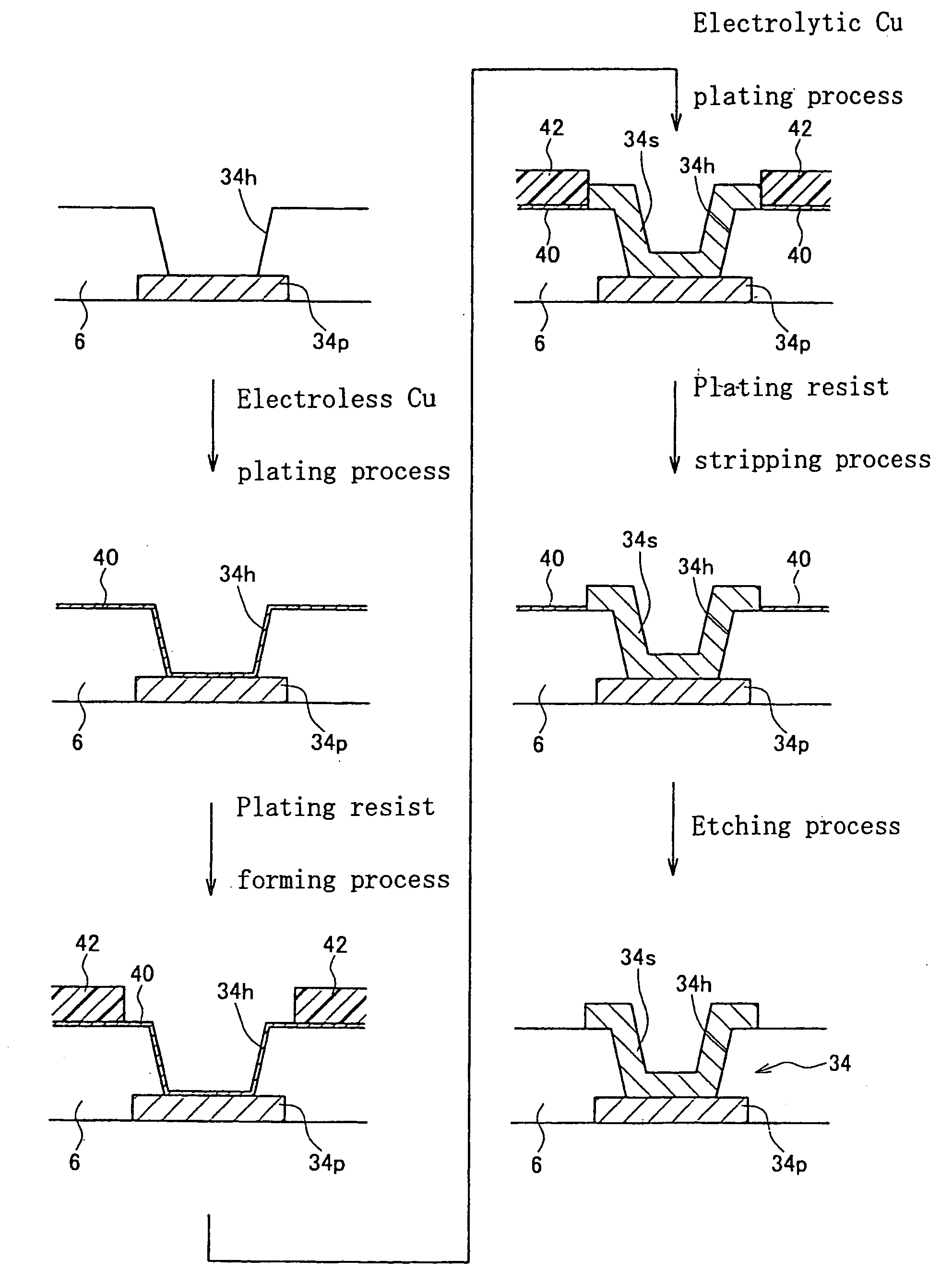
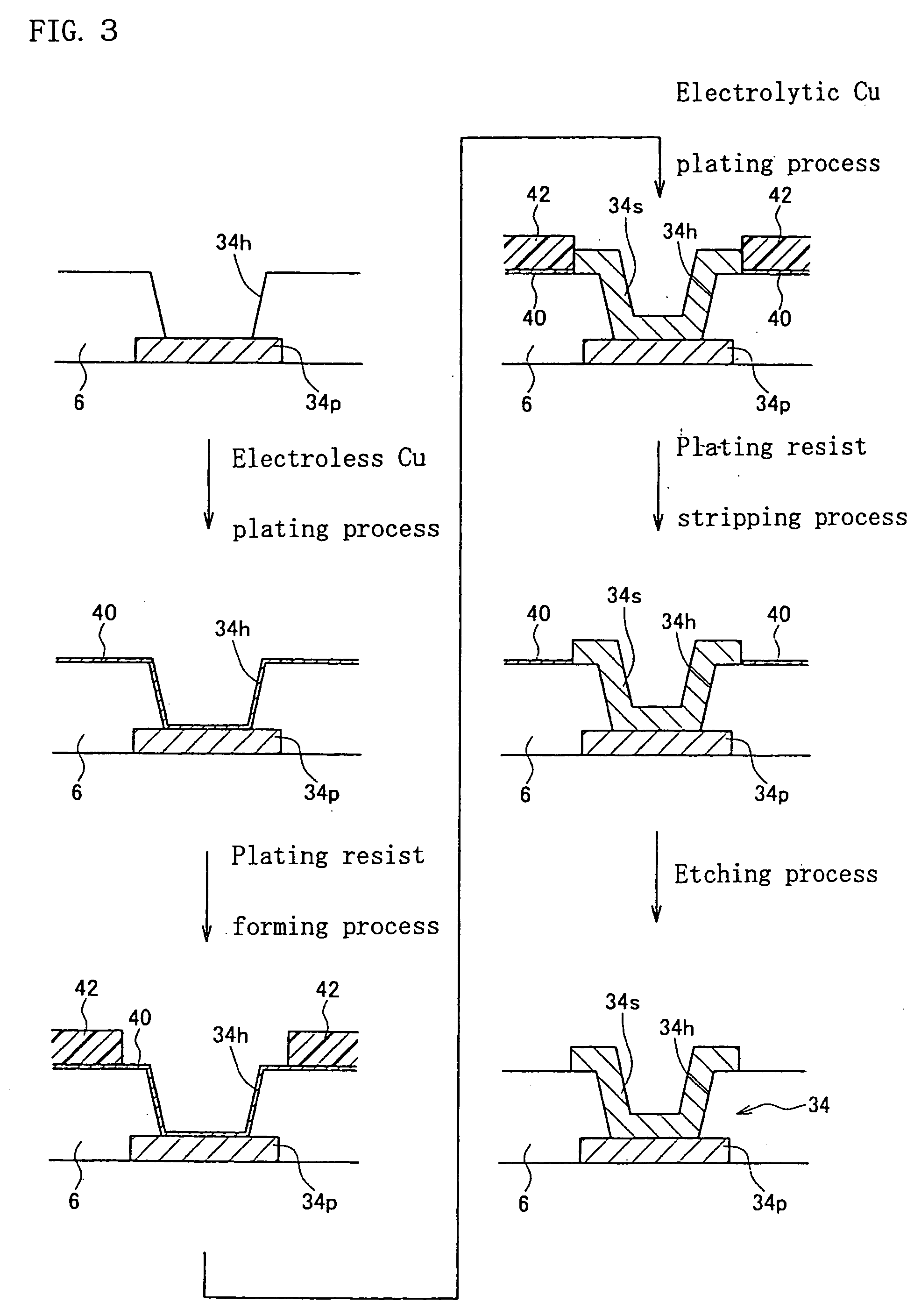
When the thickness of the electroless Cu plating film is less than the designed value, the following problems may occur.
When the electrolytic Cu plating is carried out under these circumstances, the resultant formation of the via conductor, indicated at 96, is insufficient, and a problem with there being a good electrical connection between the via conductor 96 and via pad 98 may occur.

Method used


Image

  • Manufacturing methods and electroless plating apparatus for manufacturing wiring circuit boards
  • Manufacturing methods and electroless plating apparatus for manufacturing wiring circuit boards
  • Manufacturing methods and electroless plating apparatus for manufacturing wiring circuit boards

Examples


example

[0067] The following experiment was conducted in order to confirm the effects produced by the invention.

[0068] a. The Electroless Plating Apparatus

[0069] The experiment was conducted by using an electroless plating apparatus 200 shown in a plan view in FIG. 12. The elements indicated in the thick line in the plating bath 53 is the bubble generator 57 described above in connection with FIG. 7. During the execution of the plating process, the air feeding rate at which air is fed into the bubble generator 57 was adjusted by mass flow controller (not shown).

[0070] b. The Wiring Circuit Board Workpiece

[0071] As shown in FIG. 12, the rack 51 was disposed immediately above the bubble generator 57. The wiring circuit board workpieces 100 were suspended at positions indicated by thin lines inside of the rack 51. For all of the wiring circuit board workpieces 100, the principal substrate surface extends parallel to the longitudinal direction in FIG. 12 and perpendicular to the plane of th...


PUM


Abstract

A manufacturing method for wiring circuit boards enhances product yield and promotes uniform electrical characteristics among the products by reducing fluctuations in the thickness of the electroless Cu plating film. In a plating bath (53) containing an electroless Cu plating liquid (EPL), wiring circuit board workpieces (100) are held in an upright position so as to leave gaps permitting distribution of the EPL. A bubble generator (57), which produces bubbles in the installation area of the workpieces (100), is disposed between the bottom of the bath (53) and the workpieces so as to help form an electroless Cu plating film (40) on each workpiece (100) and so that bubbles from the bubble generator (57) rise up along both sides of each workpiece.

Description

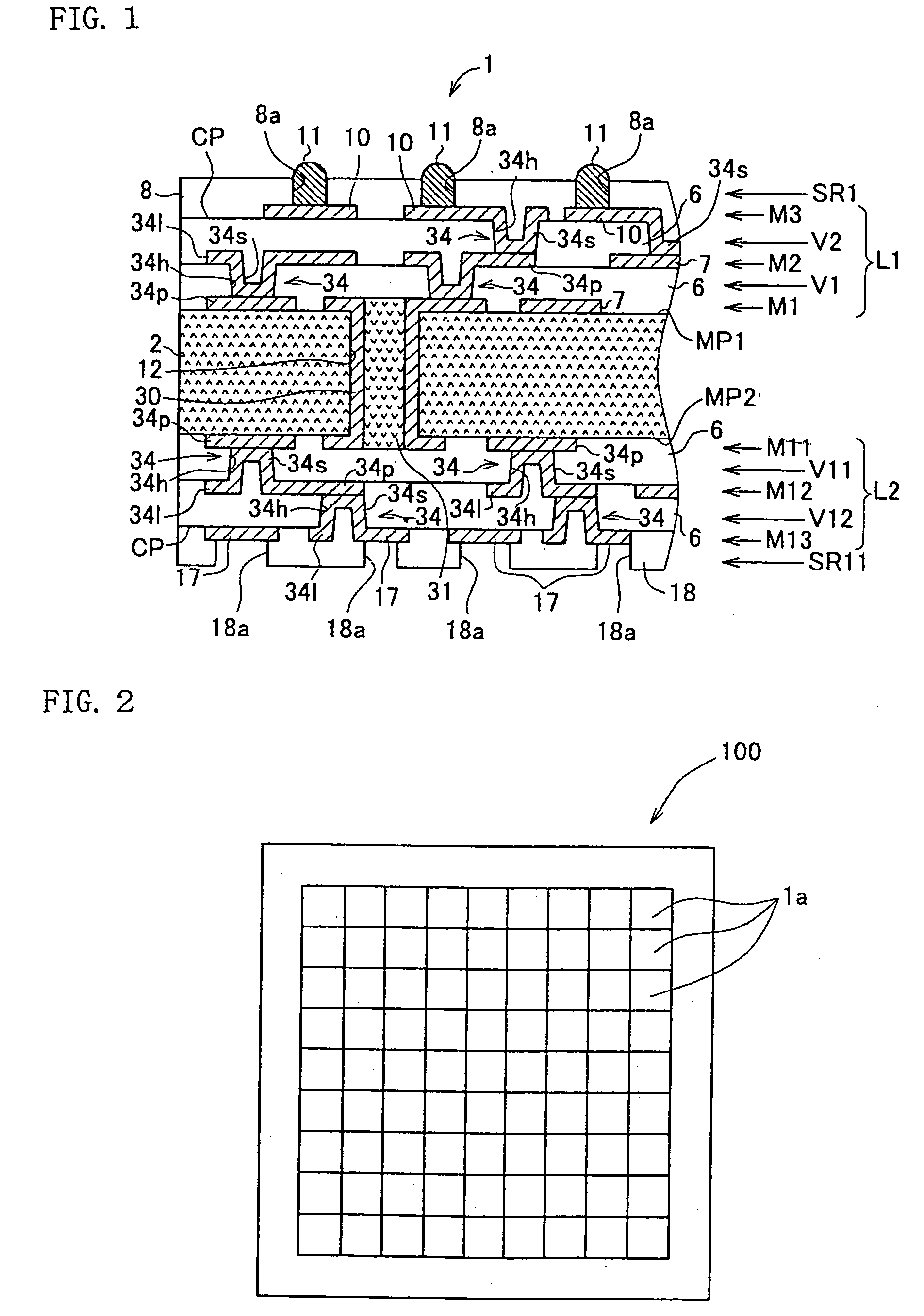
BACKGROUND OF THE INVENTION [0001] 1. Field of the Invention [0002] The present invention relates to manufacturing methods for making wiring circuit boards. More particularly, the invention relates to wiring circuit board manufacturing methods which use electroless Cu plating and to an electroless plating apparatus for manufacturing wiring circuit boards. [0003] 2. Description of the Related Art [0004] Organic wiring circuit boards having a mutually laminated structure formed by at least one dielectric layer and at least one conductor layer of high molecular weight material are well known. Such circuits are commonly referred to as multilayer wiring circuit boards and are used for connection of IC, LSI and other chips. Today, most organic wiring circuit boards having ultrafine circuits are manufactured by a “build-up” method which involves stacking a conductor layer and a dielectric layer, one by one, alternately, on a core substrate. In a typical example of the build-up method, a th...

Claims


Application Information

Patent Timeline
Patent Type & Authority Applications(United States)
IPC IPC(8): H01L21/44
CPCH05K3/108H05K3/187H05K2203/1518H05K3/422H05K2203/087H05K3/421
Inventor TOKUDA, TAKUYA
Owner NGK SPARK PLUG CO LTD
Learn More