Check patentability & draft patents in minutes with Patsnap Eureka AI!

Semiconductor packages

a technology of semiconductors and components, applied in the field of semiconductor packages, can solve the problems of negative performance properties induced, size limitations imposed by the size of the interposer,

Inactive Publication Date: 2006-03-16
KHENG LEE TECK
View PDF21 Cites 15 Cited by
  • Summary
  • Abstract
  • Description
  • Claims
  • Application Information

AI Technical Summary

Problems solved by technology

The package design of FIG. 1 can have various problems associated with the utilization of the interposer 14.
Such problems can include size limitations imposed by the size of the interposer.
The problems can also include negative performance properties induced by the interposer through, for example, adsorption of moisture by the interposer and / or outgassing of materials from the interposer.

Method used


Image

  • Semiconductor packages
  • Semiconductor packages
  • Semiconductor packages

Examples


Embodiment Construction

[0029] This disclosure of the invention is submitted in furtherance of the constitutional purposes of the U.S. Patent Laws “to promote the progress of science and useful arts” (Article 1, Section 8).

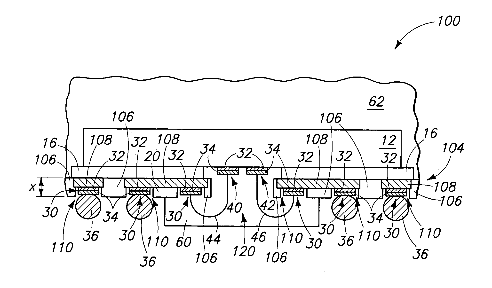
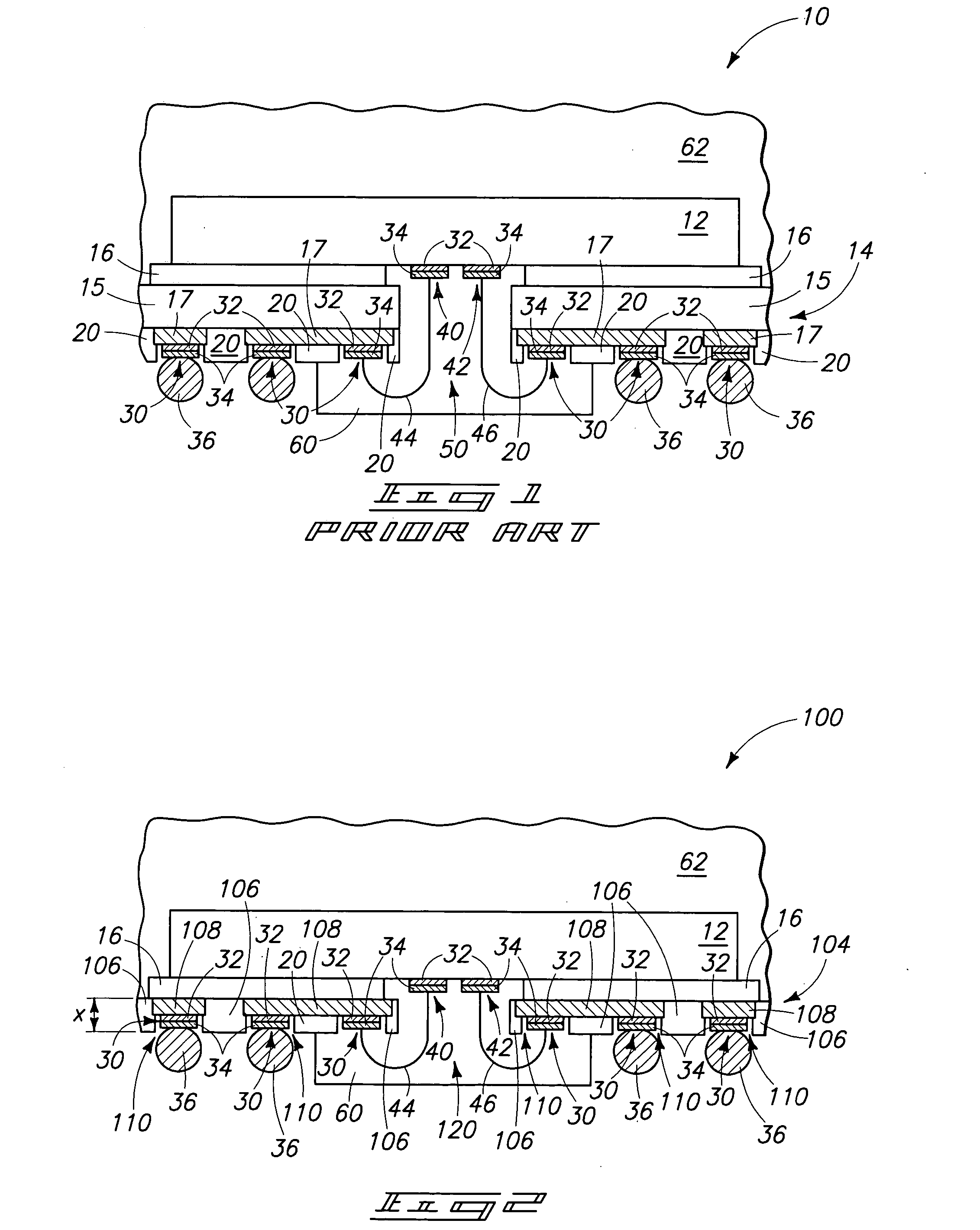
[0030] An exemplary aspect of the invention is described with reference to FIG. 2. In referring to FIG. 2, similar numbering will be used as is utilized above in describing the prior art semiconductor package of FIG. 1, where appropriate.

[0031]FIG. 2 shows a semiconductor package 100 comprising an integrated circuit die (which can also be referred to herein as a semiconductor die) 12. The die is adhered to an interposer construction 104 through an electrically insulative adhesive structure 16. The interposer 104 can be referred to as a frame carrier interposer, to emphasize that the interposer is carrying the circuit trace frame.

[0032] The interposer 104 differs from the interposer 14 of FIG. 1, in that the interposer 104 is missing the core 15 described previously. Specifically, inte...


PUM


Abstract

The invention includes semiconductor packages having a patterned substrate with openings extending therethrough, conductive circuit traces over the substrate and having portions extending over the openings, a semiconductor die over the circuit traces, and a matrix contacting the circuit traces and also contacting the die. The invention also includes methods of forming semiconductor packages. Such methods can include provision of a construction comprising an electrically conductive layer on a masking material. The layer has a first surface facing the masking material and a second surface in opposing relation to the first surface. The masking material is patterned to form openings extending to the first surface of the layer. The layer is then patterned. Subsequently, an integrated circuit die is provided over the second surface of the layer.

Description

TECHNICAL FIELD [0001] The invention pertains to semiconductor packages, and to methods of forming semiconductor packages. BACKGROUND OF THE INVENTION [0002] Semiconductor devices (for example, dynamic random access memory (DRAM) devices), are shrinking in the sense that smaller devices are being manufactured that are able to handle larger volumes of data and faster data transfer rates. Semiconductor manufacturers have been moving toward chip-scale packages (CSP) for semiconductor components having a small size and fine pitch wiring. [0003] An exemplary CSP is shown in FIG. 1 as a board-on-chip (BOC) package 10. The package comprises a semiconductor component 12, such as an integrated circuit chip (or die), and accordingly the package can be referred to as a semiconductor package. [0004] The package 10 comprises an interposer 14 utilized to support the semiconductor component 12. The shown interposer comprises a board 15, dielectric (i.e., electrically insulative) material 20 on one...

Claims


Application Information

Patent Timeline
Patent Type & Authority Applications(United States)
IPC IPC(8): H01L23/495H01L21/48H01L23/13H01L23/48H01L23/498
CPCH01L23/13H01L23/49816H01L2924/01033H01L2924/01005H01L2924/00014H01L2924/30107H01L2924/15311H01L2924/14H01L2924/014H01L23/49838H01L24/48H01L2224/0401H01L2224/05155H01L2224/05644H01L2224/48091H01L2224/4824H01L2224/484H01L2224/73215H01L2224/85444H01L2924/01028H01L2924/01029H01L2924/01046H01L2924/01078H01L2924/01079H01L2224/45099H01L2924/181H01L2924/00012
Inventor KHENG, LEE TECK
Owner KHENG LEE TECK
Features
  • R&D
  • Intellectual Property
  • Life Sciences
  • Materials
  • Tech Scout
  • Unparalleled Data Quality
  • Higher Quality Content
  • 60% Fewer Hallucinations
Learn More