Remotely communicating, battery-powered nanostructure sensor devices

a nanostructure sensor and remote communication technology, applied in the direction of electric signalling details, fire alarms, instruments, etc., can solve the problems of large amount of power, and relatively small amount of power, and achieve the effect of increasing range and low power consumption

Inactive Publication Date: 2006-03-16
NANOMIX
View PDF71 Cites 116 Cited by
  • Summary
  • Abstract
  • Description
  • Claims
  • Application Information

AI Technical Summary

Benefits of technology

The patent describes how a small sensor can communicate wirelessly with another device called a base station. This allows for more efficient use of battery power because the sensor doesn't have to constantly send data. There are also different ways for multiple sensors to work together to form a network. Overall, these features make it easier to design and develop wireless networks of sensors.

Problems solved by technology

The technical problem addressed by this patent is creating a small and affordable remote sensing device capable of operating for extended periods on a limited power supply. Current technologies make it difficult to find suitable sensors that meet these criteria, especially those that are highly specialized and require significant power.

Method used


Image

  • Remotely communicating, battery-powered nanostructure sensor devices
  • Remotely communicating, battery-powered nanostructure sensor devices
  • Remotely communicating, battery-powered nanostructure sensor devices

Examples


example a

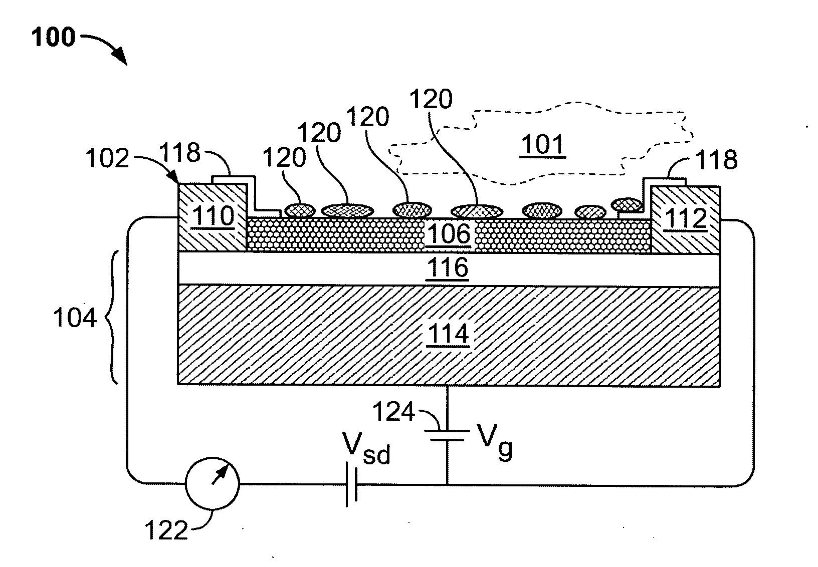
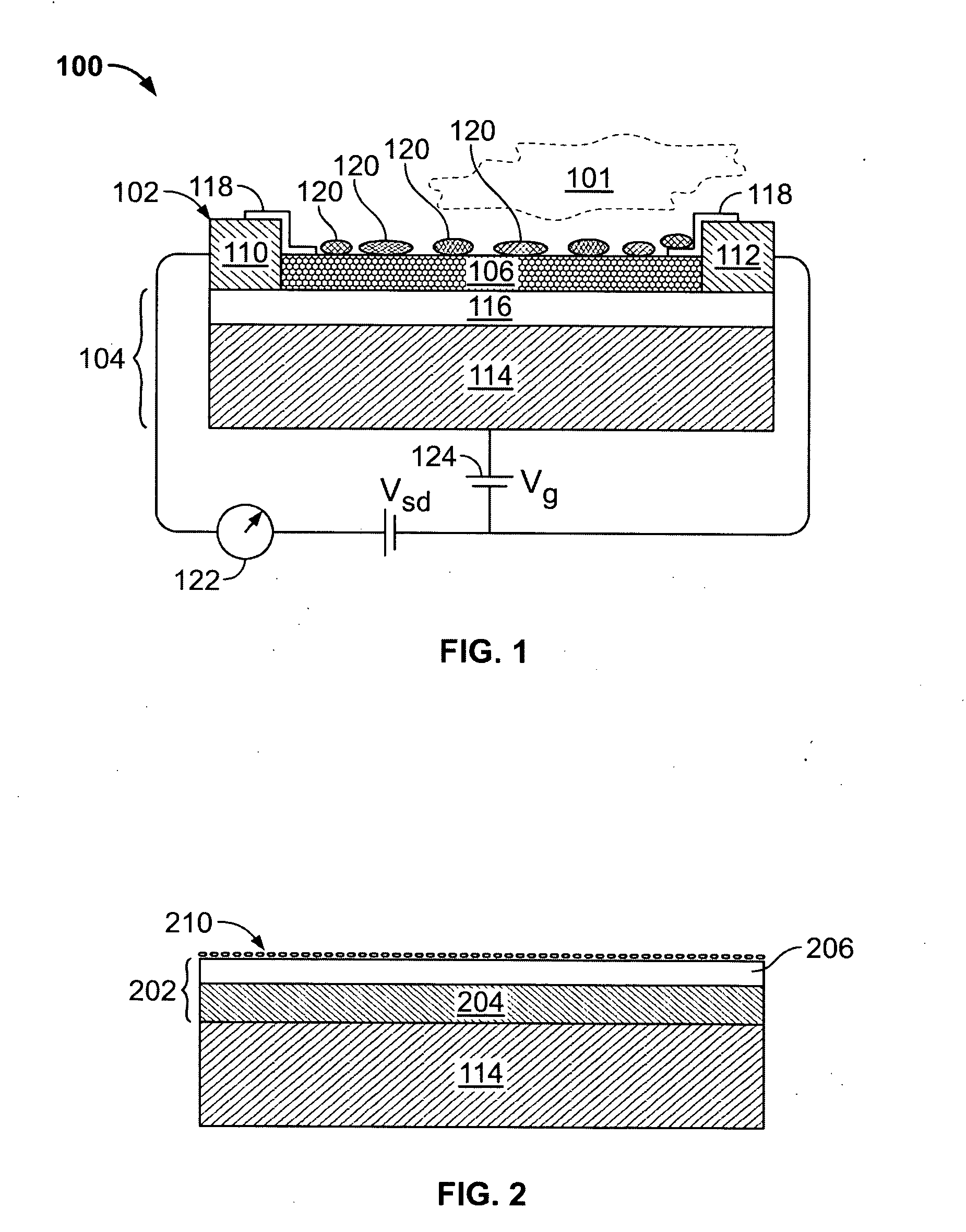
[0118] Nanotube Network CO2 Sensor with remote measurement circuitry. An exemplary NTFET H2 sensor with remote measurement circuitry was prepared as follows. A degenerately doped silicon wafer with a silicon oxide film was coated with carbon nanotubes in a random network, as described in the above-incorporated application Ser. No. 10 / 177,929. A plurality of nanosensor devices 500 were thus formed, one of which is shown schematically in FIG. 5. Titanium contacts 35 nm thick covered with gold contacts 100 nm thick were deposited and patterned by photolithography and lift-off to form opposing contacts 502, 504. Contacts 502, 504 each comprised a plurality of interdigitated portions disposed over a generally rectangular region 506. A network of randomly oriented nanotubes 508 was disposed over the silicon substrate in electrical contact with interdigitated portions of contacts 502, 504.

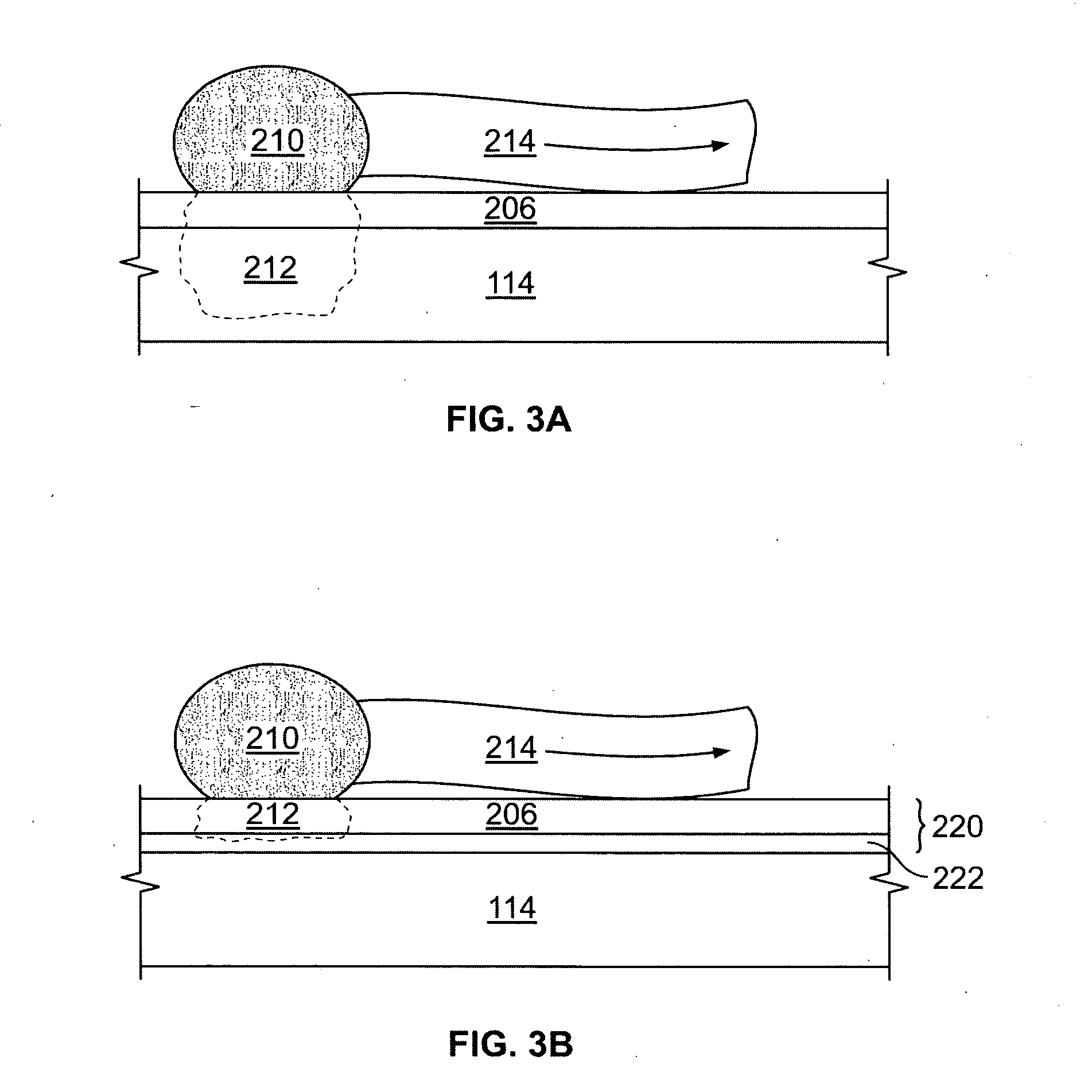
[0119] After the deposition of the contacts 502, 504 and network 508, nanotubes outside of the genera...

example b

[0125] Nanotube Network H2 Sensor with remote measurement circuitry. The process as described above in Example A, except for deposition of polyethylene imine, was carried out construct a bare (non-functionalized) nanosensor device. Over a range of gate voltages between +10 V and −10 V, the maximum conductance of the bare device was approximately 10 kΩ, and the on-off ratio was approximately 10. Many such devices were constructed on individual dies of a wafer. To functionalize for hydrogen, palladium metal was deposited on the substrate and patterned using photolithography and lift-off, as described above.

[0126] A selected die was separated from the wafer and mounted in a standard 16-pin chip carrier. Wires were used to connect leads 510, 512 to the contacts on the chip carrier, which connected to measurement circuitry on a prototype circuit board. The measurement circuit 600 was constructed as diagrammed in FIG. 7, using integrated circuit chips mounted on the same circuit board as...


PUM


Abstract

A portable sensor device incorporates a low-power, nanostructure sensor coupled to a wireless transmitter. The sensor uses a nanostructure conducting channel, such as a nanotube network, that is functionalized to respond to a selected analyte. A measurement circuit connected to the sensor determines a change in the electrical characteristic of the sensor, from which information concerning the present or absence of the analyte may be determined. The portable sensor device may include a portable power source, such as a battery. It may further include a transmitter for wirelessly transmitting data to a base station.

Description


Claims


Application Information

Patent Timeline
Owner NANOMIX
Why Eureka
Try Eureka