Printed circuit board material for embedded passive devices

a passive device and printed circuit board technology, applied in the direction of dielectric characteristics, high frequency circuit adaptations, dielectric substrate metal adhesion improvement, etc., can solve the problems of peel strength reduction, adhesion reduction, and adhesion reduction, and achieve excellent electromagnetic properties and reliability

Inactive Publication Date: 2006-03-23
SAMSUNG ELECTRO MECHANICS CO LTD
View PDF10 Cites 11 Cited by
  • Summary
  • Abstract
  • Description
  • Claims
  • Application Information

AI Technical Summary

Benefits of technology

[0011] Accordingly, an object of the present invention is to provide a printed circuit board material for embedded passive devices, which has excellent electromagnetic properties and reliability.
[0012] Another object of the present invention is to provide a printed circuit board material for embedded passive devices, which includes a resin bonding layer interposed between a conductive layer and a functional layer and is excellent in dielectric and magnetic properties and adhesion strength.

Problems solved by technology

This causes reliability problems, such as the occurrence of peeling after production.
However, an increase in the thermal resistance of resin generally causes the problem of a reduction in peel strength.
A reduction in the roughness of such metal foils improves the characteristic uniformity and etching properties, but causes the problem of a reduction in adhesion.
The three-layer RCC foil having the resin bonding layer on the filler / resin mixture layer overcomes the problem of adhesion to a surface to be adhered, which is problematic in the prior RCC foil, but both the two-layer RCC foil and the three-layer RCC foil still have the above-described problem of low peel strength between the copper foil and the resin / filler mixture layer.
However, such patents do not include any disclosure on the improvement of peel strength.
However, it also does not include any disclosure on an increase in the adhesion between the electrode layer and the dielectric layer.

Method used


Image

  • Printed circuit board material for embedded passive devices
  • Printed circuit board material for embedded passive devices
  • Printed circuit board material for embedded passive devices

Examples


##ventive example 1

INVENTIVE EXAMPLE 1

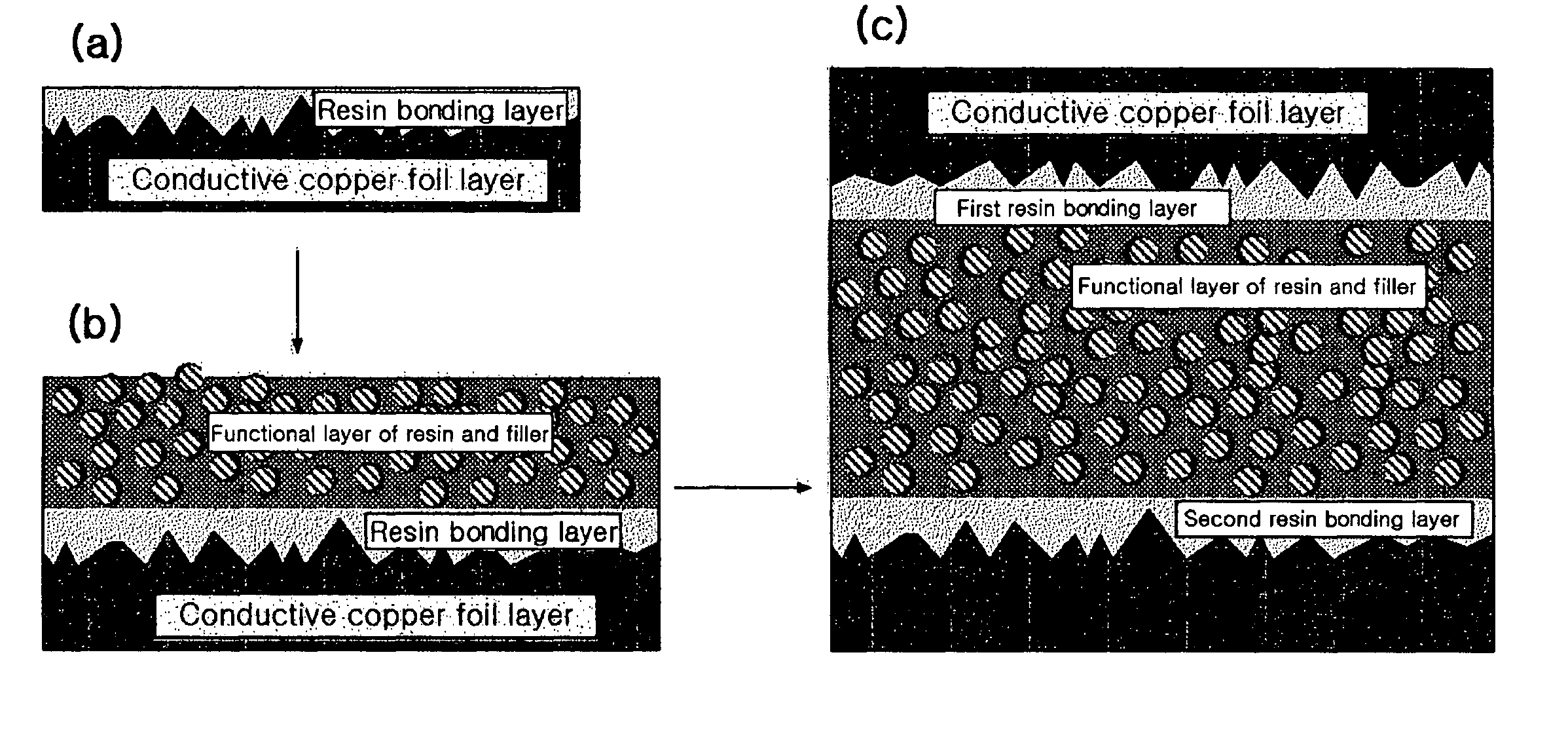
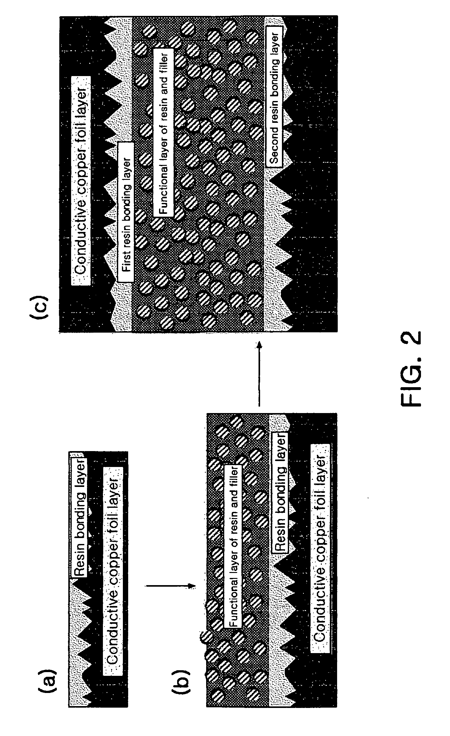
[0070] This inventive example shows that printed circuit board material samples produced according to the inventive method maintain excellent peel strength regardless of a change in the content of fillers in a functional layer. The printed circuit board material samples used for the measurement of peel strength were produced in the following manner.

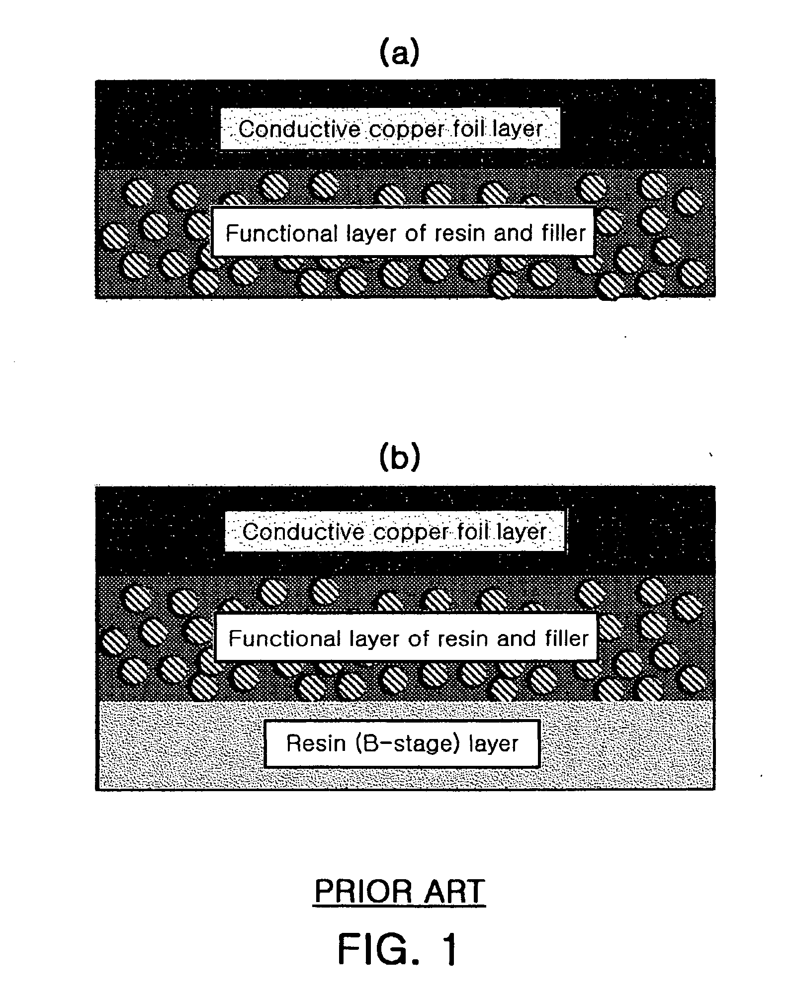
[0071] On one surface of an STD copper foil with a roughness of 5 μm and a width of 450 mm, a resin bonding layer made of bisphenol A epoxy resin was coated in a thickness of 10 μm by a comma coating method. The coated resin bonding layer was subjected to B-stage semi-curing at 150-170° C. for 1-5 minutes. Then, on the semi-cured resin bonding layer, a dielectric layer was coated in a thickness of 20 μm by a comma coating method, and subjected to B-stage semi-curing at 150-170° C. for 1-5 minutes, thus producing an RCC foil. Then, two pieces of the RCC foils produced as described above were laminated to each other in s...

##ventive example 2

INVENTIVE EXAMPLE 2

[0076] This Inventive Example shows that printed circuit board material samples produced according to the inventive method maintain excellent peel strength regardless of a change in the content of fillers in a functional layer.

[0077] The samples used in Inventive Example 2 were produced in the same manner as in Inventive Example 1 except that a VLP copper foil with a roughness (Rz) of 3 μm was used as a copper foil, and a mixture of bisphenol A epoxy resin, bisphenol A novolac epoxy resin and brominated epoxy resin which had been mixed in a weight ratio of 1:3:1 was used as the resin in the resin bonding layer and dielectric layer. The produced samples were measured for peel strength, and the measurement results are shown in Table 2 and FIG. 5.

[0078] As evident from Table 2 and FIG. 5, the inventive samples showed excellent peel strength regardless of an increase in the content of the filler barium titanate in the dielectric layer.

TABLE 2Comparison of peel str...


PUM

PropertyMeasurementUnit
roughnessaaaaaaaaaa
thicknessaaaaaaaaaa
vol %aaaaaaaaaa

Abstract

A printed circuit board material for embedded passive devices, which has excellent electromagnetic properties and reliability is provided. The invention provides a printed circuit board material comprises: a conductive copper foil layer; a resin bonding layer formed on the conductive layer and including above 70-100 vol % of resin and 0-30 vol % of filler; and a functional layer formed on the resin bonding layer and including resin and filler. The printed circuit board material has the resin bonding layer interposed between the copper foil layer and the functional layer. Thus, even when the content of fillers in the functional layer is increased, the adhesion strength between the conductive layer and the functional layer is ensured without deteriorating the properties of the functional layer, such as dielectric and magnetic properties.

Description

RELATED APPLICATIONS [0001] The present application is based on, and claims priority from, Korean Application Number 2004-76557, filed Sep. 23, 2004, the disclosure of which is hereby incorporated by reference her ein in its entirety. BACKGROUND OF THE INVENTION [0002] 1. Field of the Invention [0003] The present invention relates to a printed circuit board (PCB) material for embedded passive devices, and more particularly to a printed circuit board material for embedded passive devices, which has excellent electromagnetic properties and reliability. [0004] 2. Description of the Prior Art [0005] As electronic products have become smaller in size and more common and functional, embedded passive device technology for embedding passive devices in PCBs has recently been introduced. This technology generally utilizes a material which is either in a printed paste form or in a form where dielectric (or magnetic) fillers capable of realizing the desired characteristics are dispersed in an i...

Claims


Application Information

Patent Timeline
Patent Type & Authority Applications(United States)
IPC IPC(8): B32B3/00B32B5/16
CPCB32B7/04H05K1/0233H05K1/024H05K1/162H05K3/386H05K2201/0116Y10T428/256H05K2201/0209H05K2201/0254H05K2201/0355H05K2201/086H05K2201/09309Y10T428/24917H05K2201/0195Y10T428/249994H05K3/38H05K1/03
Inventor SOHN, SEUNG HYUNSHIN, HYO SOON
Owner SAMSUNG ELECTRO MECHANICS CO LTD
Why Eureka
Try Eureka