

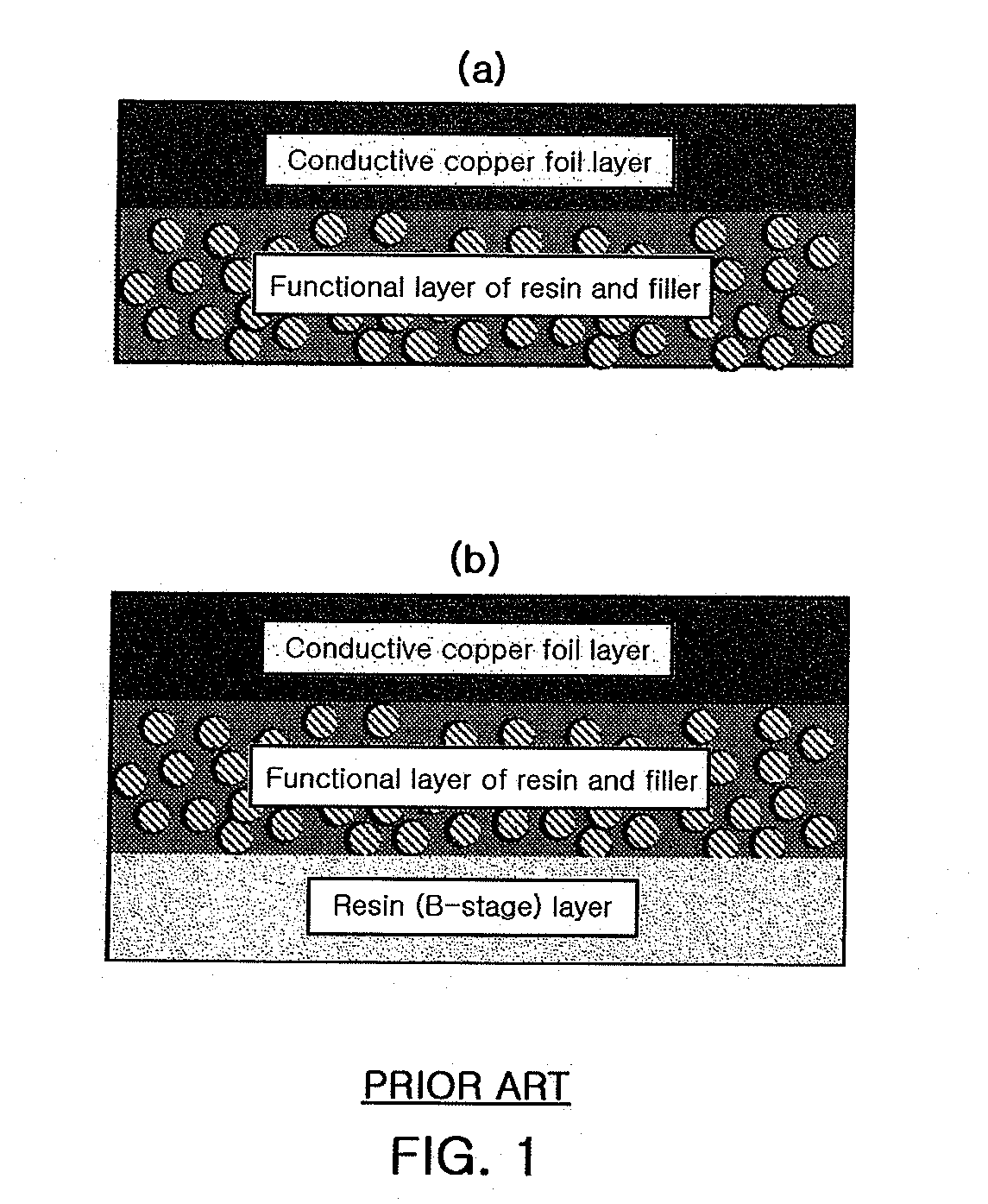
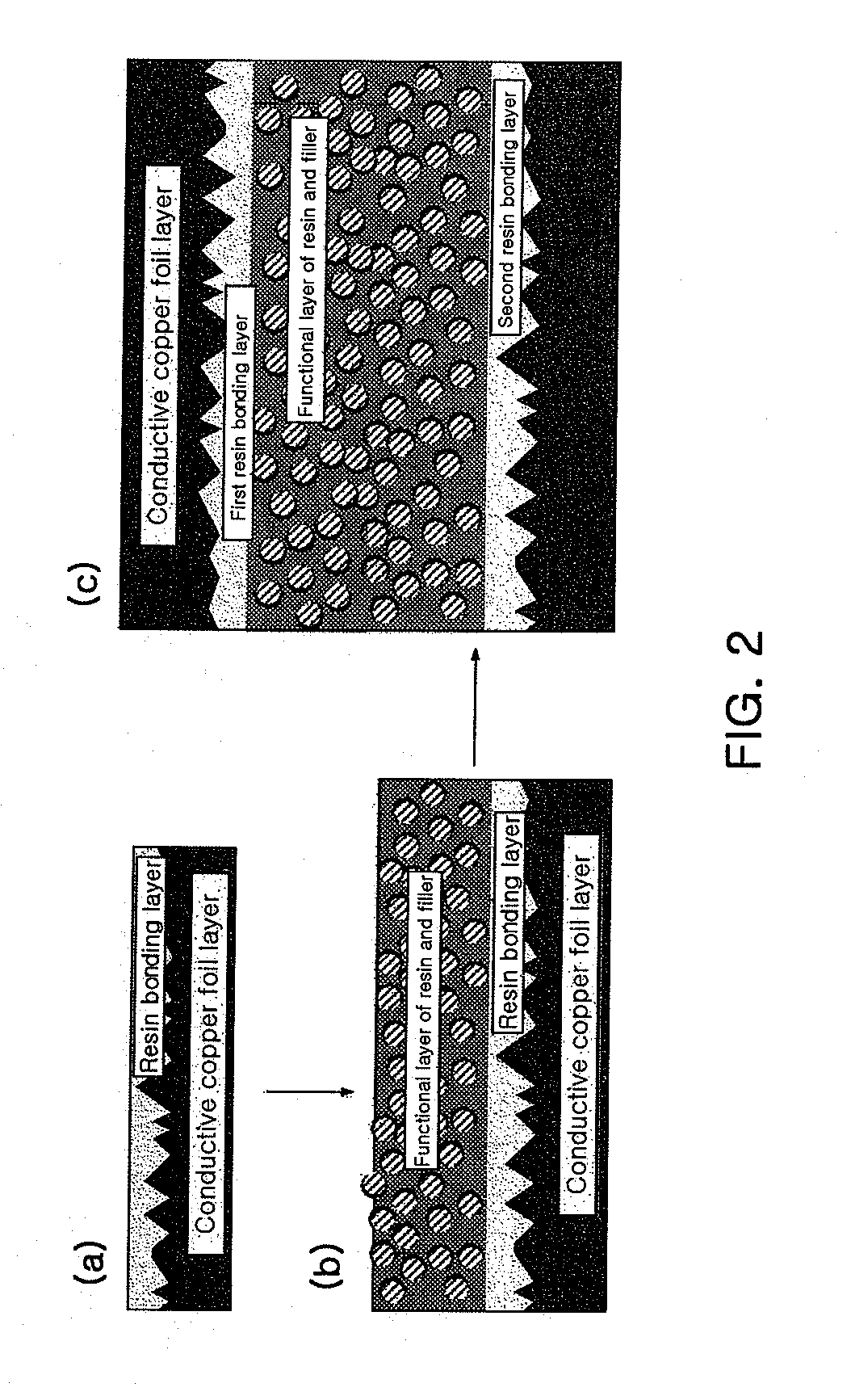
Printed circuit board material for embedded passive devices and preparing method thereof
a passive device and printed circuit board technology, applied in the direction of resistive material coating, porous dielectrics, metallic material coating processes, etc., can solve the problems of peel strength reduction, adhesion reduction, and adhesion reduction, and achieve excellent electromagnetic properties and reliability
- Summary
- Abstract
- Description
- Claims
- Application Information
AI Technical Summary
Benefits of technology
Problems solved by technology
Method used
Image

Examples
##ventive example 1
INVENTIVE EXAMPLE 1
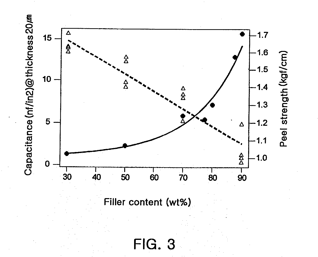
[0087] This inventive example shows that printed circuit board materials having the resin bonding layer made of a resin and a filler has improved adhesiveness between the functional layer and the conductive layer and enhanced capacitance compared with printed circuit board materials having the resin bonding layer made of a resin only.
[0088] The samples used in Inventive Example 1 were produced in the same manner as in Comparative Example 4 except that the resin bonding layers are formed with a mixture of 15 vol % of barium titanate(BaTiO3) and 85 vol % of bisphenol A epoxy rein.
[0089] The produced samples were measured for peel strength and capacitance as in comparative example 1 and the results are shown in Table 3.
TABLE 3Peel Strength and Capacitance of Inventive Example 1Filler solidsPeel strengthCapacitance(wt %)(vol %)(kgf / cm)(nF / in2)4011.61.8243.4215016.41.7943.9986022.81.8225.6247031.51.81011.2548044.01.65813.6589063.91.45127.995
[0090] As shown in the T...
##ventive example 2
INVENTIVE EXAMPLE 2
[0091] This inventive example shows that printed circuit board materials having the resin bonding layer made of a resin and a filler has improved adhesiveness between functional layer and the conductive layer and enhanced capacitance compared with printed circuit board materials having the resin bonding layer made of a resin only.
[0092] The samples used in Inventive Example 2 were produced in the same manner as in Comparative Example 4 except that the resin bonding layers are formed with a mixture of 15vol % of barium titanate(BaTiO3) and 85 vol % of resin mixture of bisphenol A epoxy resin, bisphenol A novolac epoxy resin and brominated epoxy resin which had been mixed in a weight ratio of 1:3:1.
[0093] The produced samples were measured for peel strength and capacitance as in Comparative Example 1 and the results are shown in Table 4.
TABLE 4Peel Strength and Capacitance of InventiveExample 2FillersolidsPeel strengthCapacitance(wt %)(vol %)(kgf / cm)(nF / in2)4011...
PUM
| Property | Measurement | Unit |
|---|---|---|
| roughness | aaaaa | aaaaa |
| thickness | aaaaa | aaaaa |
| thickness | aaaaa | aaaaa |
Abstract
Description
Claims
Application Information