
Organic electroluminescent device

an electroluminescent device and organic technology, applied in the field of organic electroluminescent devices, can solve the problems of low quantum efficiency of devices, need of further improvement, and devices having phosphorescent materials that are unsatisfactory in durability

Inactive Publication Date: 2006-04-06
UDC IRELAND
View PDF5 Cites 41 Cited by
  • Summary
  • Abstract
  • Description
  • Claims
  • Application Information

AI Technical Summary

Benefits of technology

[0032]<21> The organic electroluminescent device according to the above <1> to <14>, wherein the luminescent layer contains two or more of the metal complexes.

Problems solved by technology

These devices, however, have low quantum efficiencies and therefore are in need of further improvement.
However, these devices having phosphorescent materials are unsatisfactory in durability and therefore are in need of further improvement.
Also, conventional platinum complexes have the problem that the luminescent color of these platinum complexes is limited to a range from orange to red and emission of short-wavelength light of a range from blue to green which is required in applications such as a full-color or multicolor display cannot be obtained.
However, these materials are unsatisfactory in durability.
However, the devices using these materials are still unsatisfactory in durability.

Method used


Image

  • Organic electroluminescent device
  • Organic electroluminescent device
  • Organic electroluminescent device

Examples


example 1

[0197] A luminescent device is manufactured in the same manner as in Comparative Example 1 except that Ir(ppy)3 in the luminescent layer in Comparative Example 1 is altered to the complex K-9 of the invention and evaluated in the same method as in Comparative Example 1.

[0198] Green light emission (526 nm) is observed and the external quantum efficiency (η1000) at a luminance of 1,000 cd / m2 is 12%. The device is allowed to emit light successively at an initial luminance of 1,000 cd / m2 to find the time (half-value period of luminance) required for the initial luminance to be decreased to 500 cd / M2 and as a result, the time is found to be about 180 hours.

example 2

[0199] A luminescent device is manufactured in the same manner as in Comparative Example 1 except that Ir(Ppy)3 in the luminescent layer in Comparative Example 1 is altered to the complex K-19 of the invention and evaluated in the same method as in Comparative Example 1.

[0200] Blue light emission is observed and the external quantum efficiency (η1000) at a luminance of 1,000 cd / m2 is 7%. The device is allowed to emit light successively at an initial luminance of 1,000 cd / m2 to find the time (half-value period of luminance) required for the initial luminance to be decreased to 500 cd / m2 and as a result, the time is found to be about 170 hours.

example 3

[0201] A luminescent device is manufactured in the same manner as in Comparative Example 1 except that Ir(ppy)3 in the luminescent layer in Comparative Example 1 is altered to the complex K-43 of the invention and evaluated in the same method as in Comparative Example 1.

[0202] Blue light emission is observed and the external quantum efficiency (η1000) at a luminance of 1,000 cd / m2 is 5%. The device is allowed to emit light successively at an initial luminance of 1,000 cd / m2 to find the time (half-value period of luminance) required for the initial luminance to be decreased to 500 cd / M2 and as a result, the time is found to be about 200 hours.


PUM

PropertyMeasurementUnit
maximum wavelengthaaaaaaaaaa
wavelengthaaaaaaaaaa
temperatureaaaaaaaaaa

Abstract

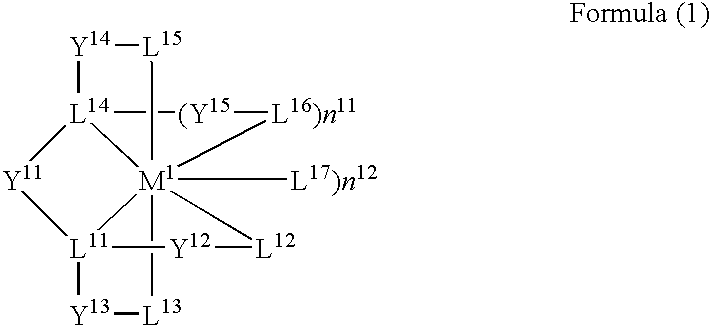
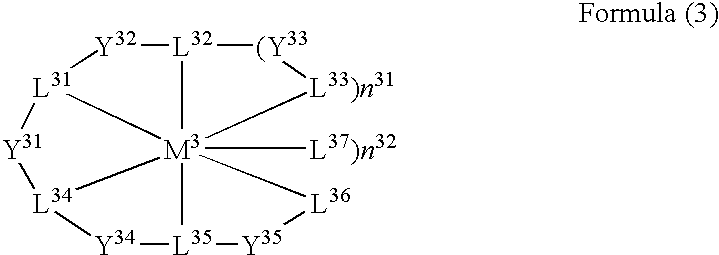
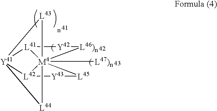
Disclosed is an organic electroluminescent device including at least one organic layer containing a luminescent layer between a pair of electrodes, wherein the organic layer contains at least one metal complex having a ligand with five or more coordination atoms.

Description

CROSS-REFERENCE TO RELATED APPLICATION [0001] This application claims priority under 35 USC 119 from Japanese Patent Application Nos. 2004-282163, the disclosure of which is incorporated by reference herein. BACKGROUND OF THE INVENTION [0002] 1. Field of the Invention [0003] The present invention relates to a luminescent device and particularly, to an organic electroluminescent device (EL device). [0004] 2. Description of the Related Art [0005] Active research is ongoing to develop various display devices, among which organic electroluminescent (EL) devices attract remarkable attention as promising display devices because high luminance emission is obtained from these devices at a low voltage. Durability is among the important characteristics of organic EL devices, and trials are being made to improve the durability of these organic EL devices. As measures to improve the durability, luminescent devices using CuPc (copper phthalocyanine) in a hole injecting layer are known (see, for ...

Claims


Application Information

Patent Timeline
Patent Type & Authority Applications(United States)
IPC IPC(8): B32B19/00
CPCC07F15/0033C07F15/004C07F15/0073C07F15/0093C07F15/065H01L51/0081H01L51/0084H01L51/0085H01L51/0086H01L51/0087H10K85/341H10K85/344H10K85/324H10K85/346H10K85/342
Inventor ISE, TOSHIHIROOKADA, HISASHIMURAKAMI, TAKESHIICHIJIMA, SEIJI
Owner UDC IRELAND
Learn More