
Optical module
- Summary
- Abstract
- Description
- Claims
- Application Information
AI Technical Summary
Benefits of technology
Problems solved by technology
Method used
Image

Examples
first embodiment
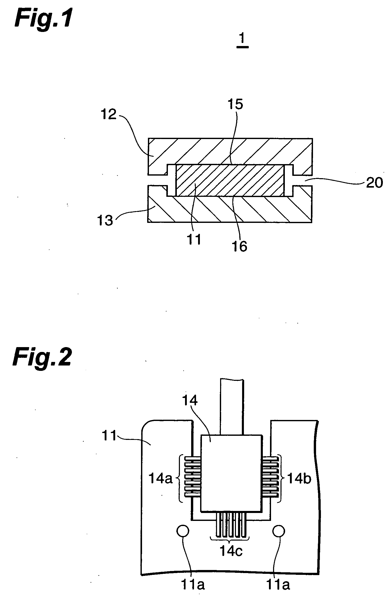
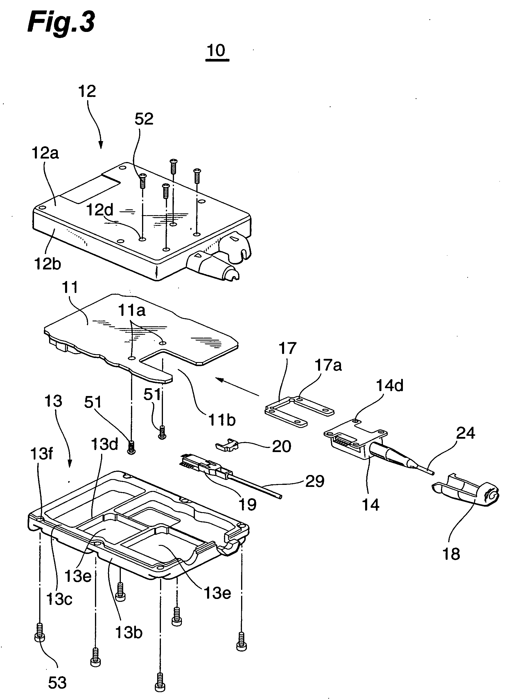
[0046] In the following, the structure of the optical module 10 in accordance with the first embodiment will be explained in detail with reference to FIGS. 3 to 5. FIG. 3 is an exploded perspective view of the optical module 10 as looked down from the upper housing 12 side. FIG. 4 is an exploded perspective view of the optical module 10 as looked up from the lower housing 13 side. FIG. 5 is a sectional view of the optical module 10.
[0047] The optical module 10 is a transmitter / receiver for optical communications. The optical module 10 comprises a substrate 11, an upper housing 12, and a lower housing 13. An LD module 14, a Pin AMP 19, and other components (a control circuit, an electrical connector 21, etc.) are mounted on the front face of the substrate 11. The LD module 14 is a light-emitting module, whereas the Pin AMP 19 is a light-receiving module. The LD module 14 incorporates a laser diode therein. The Pin AMP 19 incorporates a photodiode therein. The LD module 14 includes a...
second embodiment
[0068] A second embodiment of the present invention will now be explained. Constituents identical to those explained in the above-mentioned first embodiment will be referred to with numerals identical thereto without repeating their overlapping descriptions.
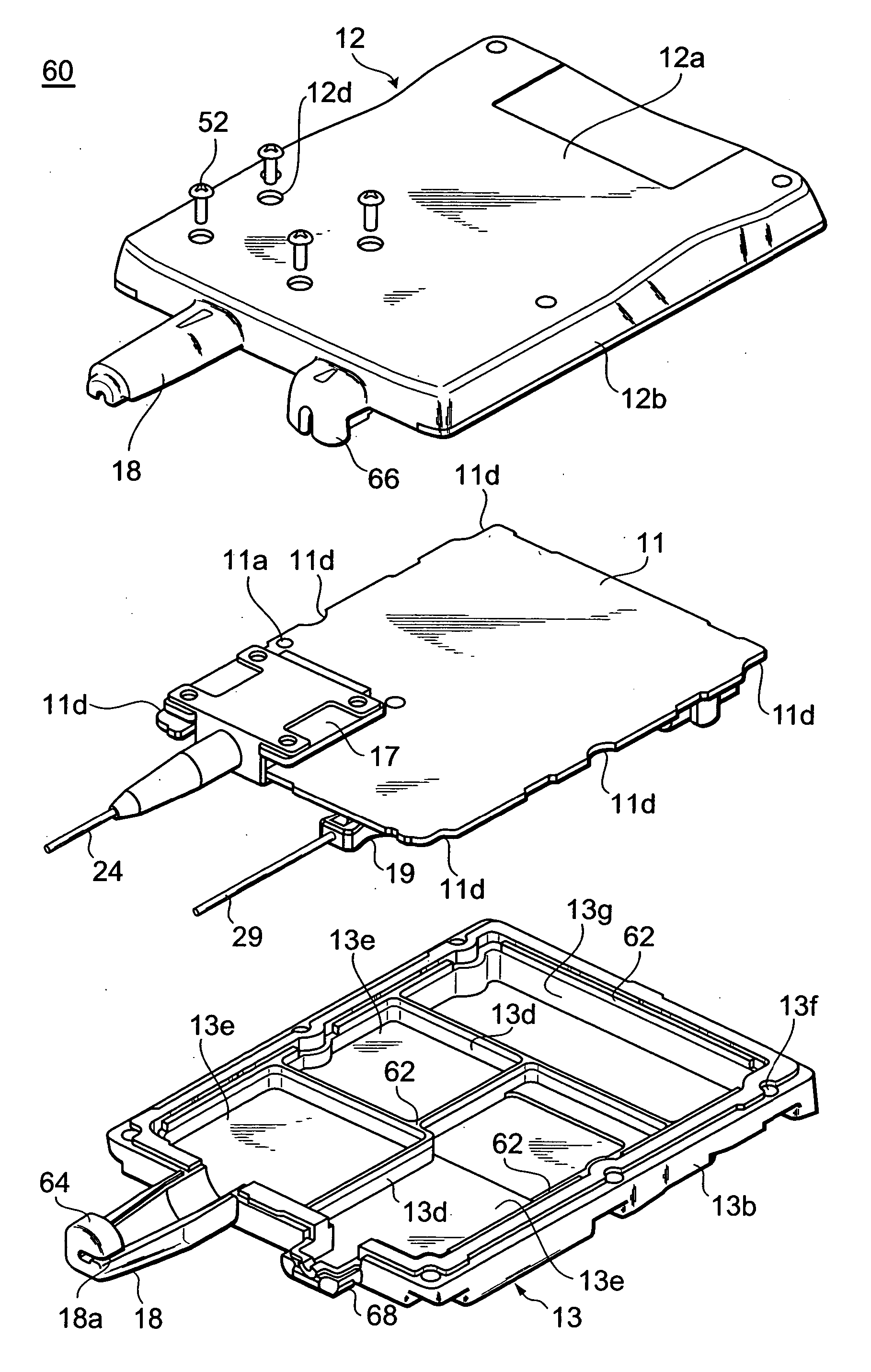
[0069]FIG. 14 is a perspective view showing the configuration of the optical module in accordance with the second embodiment. FIGS. 15 and 16 are exploded perspective views showing the configuration of the optical module in accordance with the second embodiment.
[0070] As shown in FIGS. 14 to 16, this optical module 60 comprises an LD module 14, a Pin AMP 19, a semiconductor circuit device 23, an electrical connector 21, a substrate 11, a housing (an upper housing 12 and a lower housing 13), etc.
[0071] As shown in FIG. 15, the LD module 14 is a module of butterfly package type as with the LD module in the optical module 10 in accordance with the above-mentioned first embodiment.
[0072] As shown in FIG. 15, the Pin AMP 19 is a s...
third embodiment
[0091] The third embodiment of the present invention will now be explained. Constituents identical to those explained in the above-mentioned first and second embodiments will be referred to with numerals identical thereto without repeating their overlapping descriptions.
[0092] In the optical modules 10, 60 of the above-mentioned first and second embodiments, the upper housing 12 and lower housing 13 are connected to each other by being fastened with the six screws 53. In the optical module 80 of the third embodiment, by contrast, the upper housing 12 and lower housing 13 are held by clips 82 instead of screwing, so as to be connected to each other. On the basis of the optical module 60 in accordance with the second embodiment, the optical module 80 of the third embodiment will now be explained.
[0093]FIG. 21 is a perspective view showing the optical module 80 in accordance with the third embodiment. FIG. 22 is a perspective view showing the optical module 60 in a state free of the ...
PUM
 Abstract
Description
Claims
Application Information