

High quality large area bulk non-polar or semipolar gallium based substrates and methods
a gallium based substrate and large area technology, applied in the direction of oxide conductors, non-metal conductors, conductors, etc., can solve the problems of increased defects, thermal expansion mismatch, impurities, tilt boundaries, etc., and achieve cost-effective, cost-effective manufacturing, the effect of a large substrate area
- Summary
- Abstract
- Description
- Claims
- Application Information
AI Technical Summary
Benefits of technology
Problems solved by technology
Method used
Image

Examples
Embodiment Construction
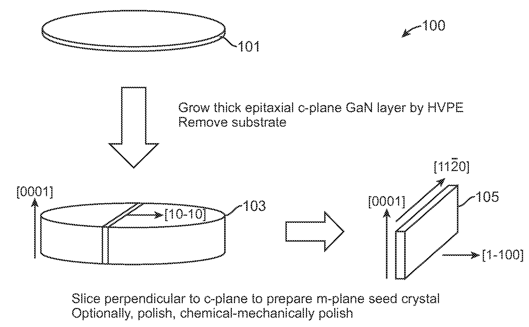
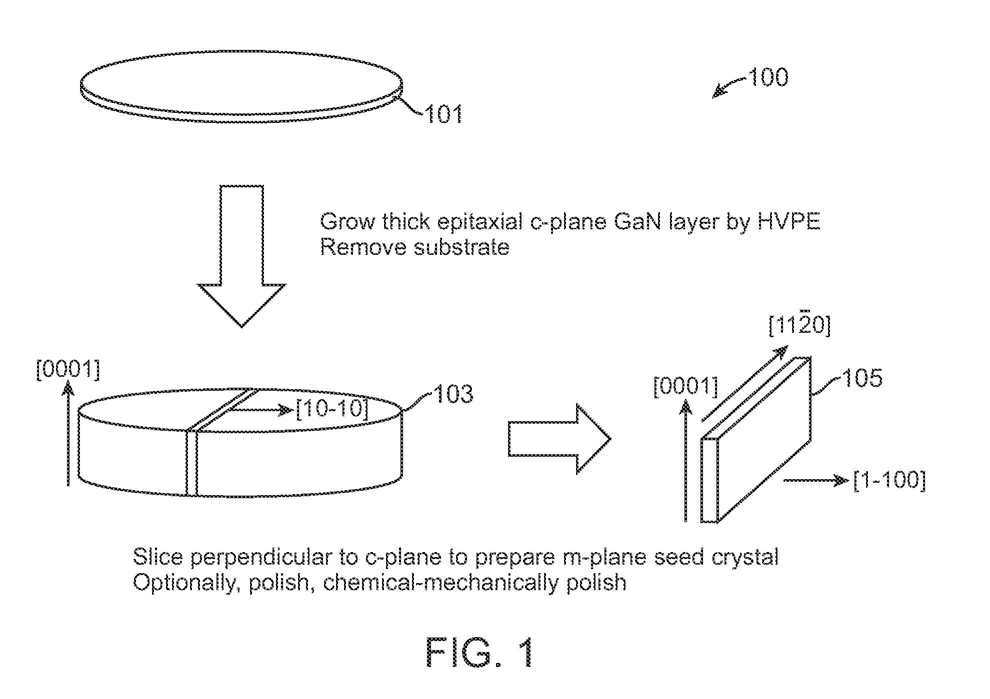
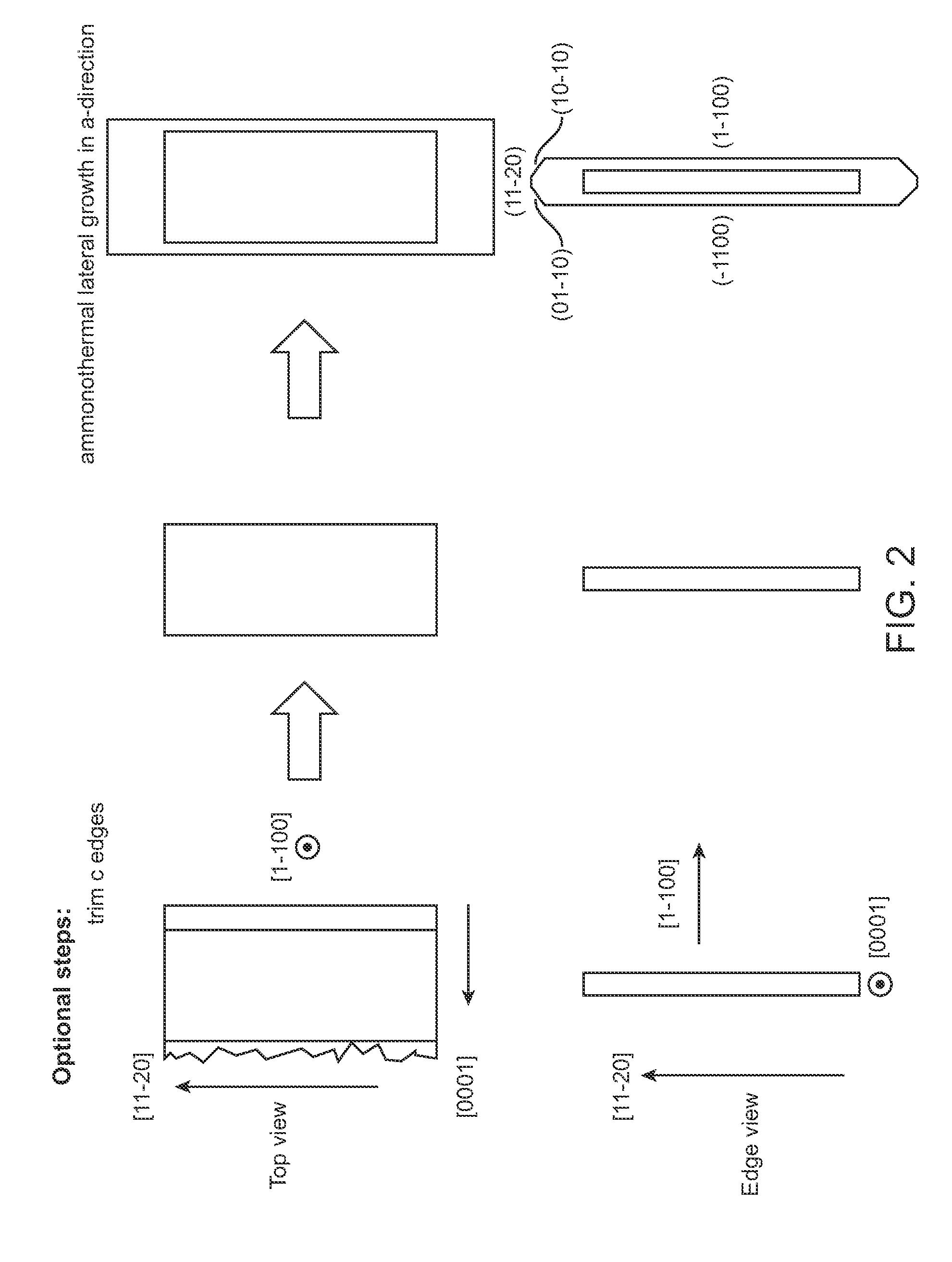
[0032]According to the present invention, techniques related to techniques for processing materials for manufacture of gallium based substrates are provided. More specifically, embodiments of the invention include techniques for growing large area substrates using a combination of processing techniques. Merely by way of example, the invention can be applied to growing crystals of GaN, AlN, InN, InGaN, AlGaN, and AlInGaN, and others for manufacture of bulk or patterned substrates. Such bulk or patterned substrates can be used for a variety of applications including optoelectronic devices, lasers, light emitting diodes, solar cells, photo electrochemical water splitting and hydrogen generation, photodetectors, integrated circuits, and transistors, and others.
[0033]FIG. 1 is a simplified diagram 100 illustrating a method for forming a GaN substrate using HVPE according to a specific embodiment of the present invention. This diagram is merely an illustration and should not unduly limit ...
PUM
| Property | Measurement | Unit |
|---|---|---|
| thickness | aaaaa | aaaaa |
| length | aaaaa | aaaaa |
| thickness | aaaaa | aaaaa |
Abstract
Description
Claims
Application Information