

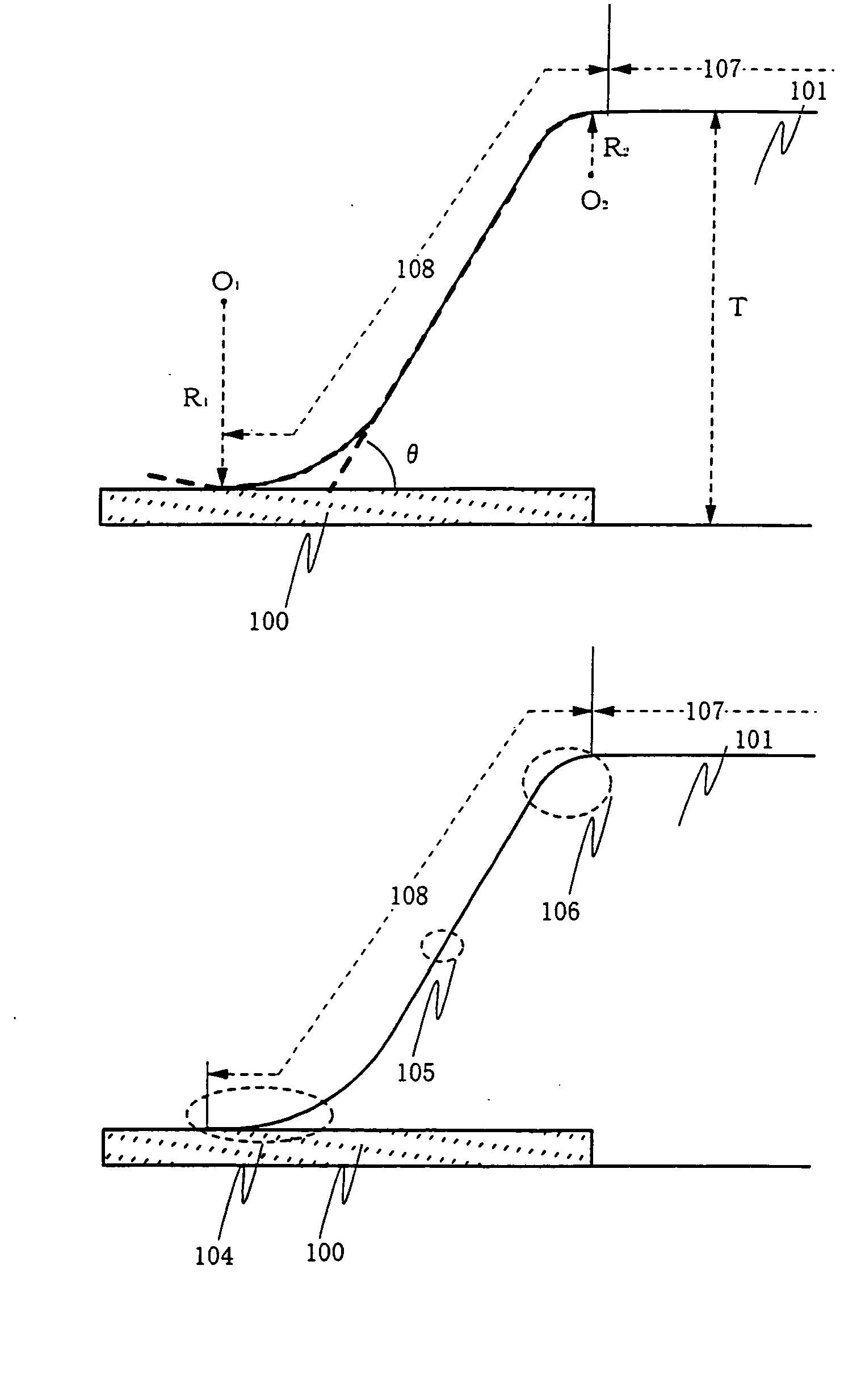
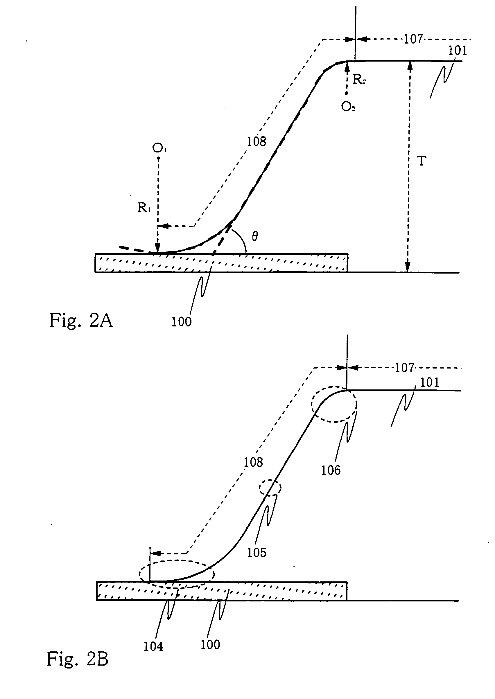
Display device and method of fabricating the display device
a display device and display device technology, applied in the field of display devices, can solve the problems of reducing yield or image quality, unable to apply the display potential to the cathode, and unable to achieve the effect of preventing discontinuity in el film or electrode, and forming the film forming surface smoothly
- Summary
- Abstract
- Description
- Claims
- Application Information
AI Technical Summary
Benefits of technology
Problems solved by technology
Method used
Image

Examples
embodiment 1
[0117] The present invention can be applied to all display devices using EL elements. FIG. 8 shows an example of a display device using EL elements, which is an active matrix display device fabricated by using TFTs. TFTs may be separated into amorphous silicon TFTs and polysilicon TFTs according to the semiconductor film material for forming the channel forming region. However, the present invention can be applied to either of display devices using amorphous silicon TFTs and display devices using polysilicon TFTs.
[0118]FIG. 8 shows a state where an n-channel TFT 452 and a p-channel TFT 453 are formed in a drive circuit portion 450, and a switching TFT 454 and a current control TFT 455 are formed in a pixel portion 451. These TFTs are formed by using semiconductor layer lands 403 to 406, gate insulating film 407, gate electrodes 408 to 411, etc.
[0119] A substrate formed of glass such as barium borosilicate glass or alumino borosilicate glass typified by #7059 glass or #1737 glass f...
embodiment 2
[0144]FIG. 13 shows an example of a display device using inverse staggered TFTs. A substrate 501 and EL elements 556 used in this embodiment are the same as those of Embodiment 1, and the description for them will not be repeated.
[0145] In the inverse staggered TFTs, gate electrodes 508 to 511, gate insulating film 507, and semiconductor films 503 to 506 are formed in this order on the substrate 501. As shown in FIG. 13, n-channel TFT 552 and p-channel TFT 553 are formed in a drive circuit portion 550, and switching TFT 554, current control TFT 555 and EL element 556 are formed in a pixel portion 551. An interlayer insulating film is formed of an inorganic insulating film 518 formed by silicon nitride, silicon oxynitride or the like and an organic insulating film 519 formed by acrylic, polyimide or the like.
[0146] The drive circuit portion 550 has different circuit configurations with respect to a gate signal drive circuit and a data signal drive circuit. The difference therebetwe...
embodiment 3
[0151] An example of an electronic device using the display device described above as Embodiment 1 will be described with reference to FIG. 14. In the display device shown in FIG. 14, TFTs formed on a substrate constitute a pixel portion 921 having pixel portion 920, a data signal drive circuit 915 used to drive the pixel portion, and a gate signal drive circuit 914. The data signal drive circuit 915 is shown as an example of a digital drive and is constituted by a shift register 916, latch circuits 917 and 918, and a buffer circuit 919. The gate signal drive circuit 914 has a shift register, a buffer, etc., (each not shown).
[0152] The pixel portion 921 has 640 (in horizontal direction)×480 (in vertical direction) pixel portion if it is of the Video Graphics Array (VGA) type. As described above with reference to FIG. 8 or FIGS. 9A and 9B, a switching TFT and a current control TFT are provided in each pixel portion. Each EL element operates in such a manner that when the gate wiring...
PUM
 Abstract
Description
Claims
Application Information