Damascene gate field effect transistor with an internal spacer structure

a gate field effect transistor and internal spacer technology, applied in the direction of semiconductor devices, transistors, electrical devices, etc., can solve the problems of frequently incompatible material options with conventional high-temperature front end of line processing, and achieve the effect of improving device performan

Inactive Publication Date: 2006-05-04
GLOBALFOUNDRIES INC
View PDF13 Cites 90 Cited by
  • Summary
  • Abstract
  • Description
  • Claims
  • Application Information

AI Technical Summary

Benefits of technology

[0004] The invention relates to a MOSFET with improved device performance and method of fabricating the device. The MOSFET comprises a source extension, a source contact disposed on the source extension, a drain extension, a drain contact disposed on the drain extension, a channel between the source extension and the drain extension, a dielectric layer above the channel, a gate spacer structure disposed on a peripheral portion of a top surface of the dielectric layer and having an internal surface that meets the top surface of the dielectric layer at about a right angle. A gate, which is disposed over a non-peripheral portion of the top surface of the dielectric layer, has at least a lower portion surrounded by and in contact with the internal surface of the gate spacer structure. The gate is also substantially aligned at its bottom with the channel.

Problems solved by technology

These material options are frequently incompatible with conventional high-temperature front end of the line processing, so that replacement gate methods are being tried where the Hi-K dielectric and the metal are deposited in a groove formed by removing a dummy gate.

Method used


Image

  • Damascene gate field effect transistor with an internal spacer structure
  • Damascene gate field effect transistor with an internal spacer structure
  • Damascene gate field effect transistor with an internal spacer structure

Examples


Embodiment Construction

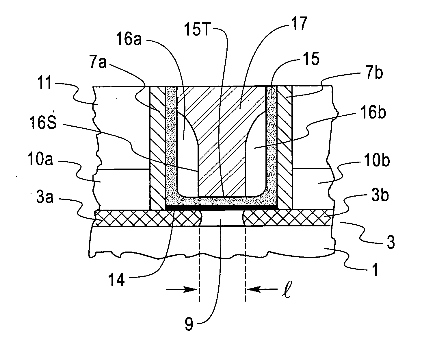
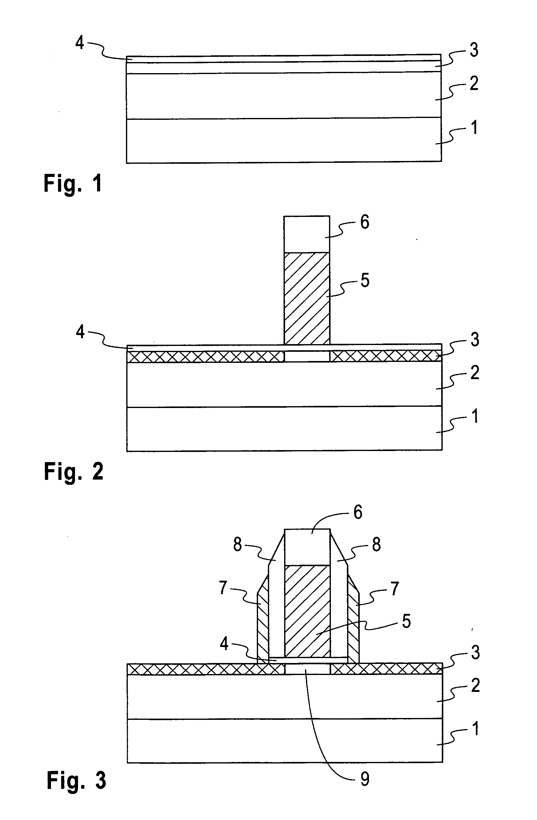
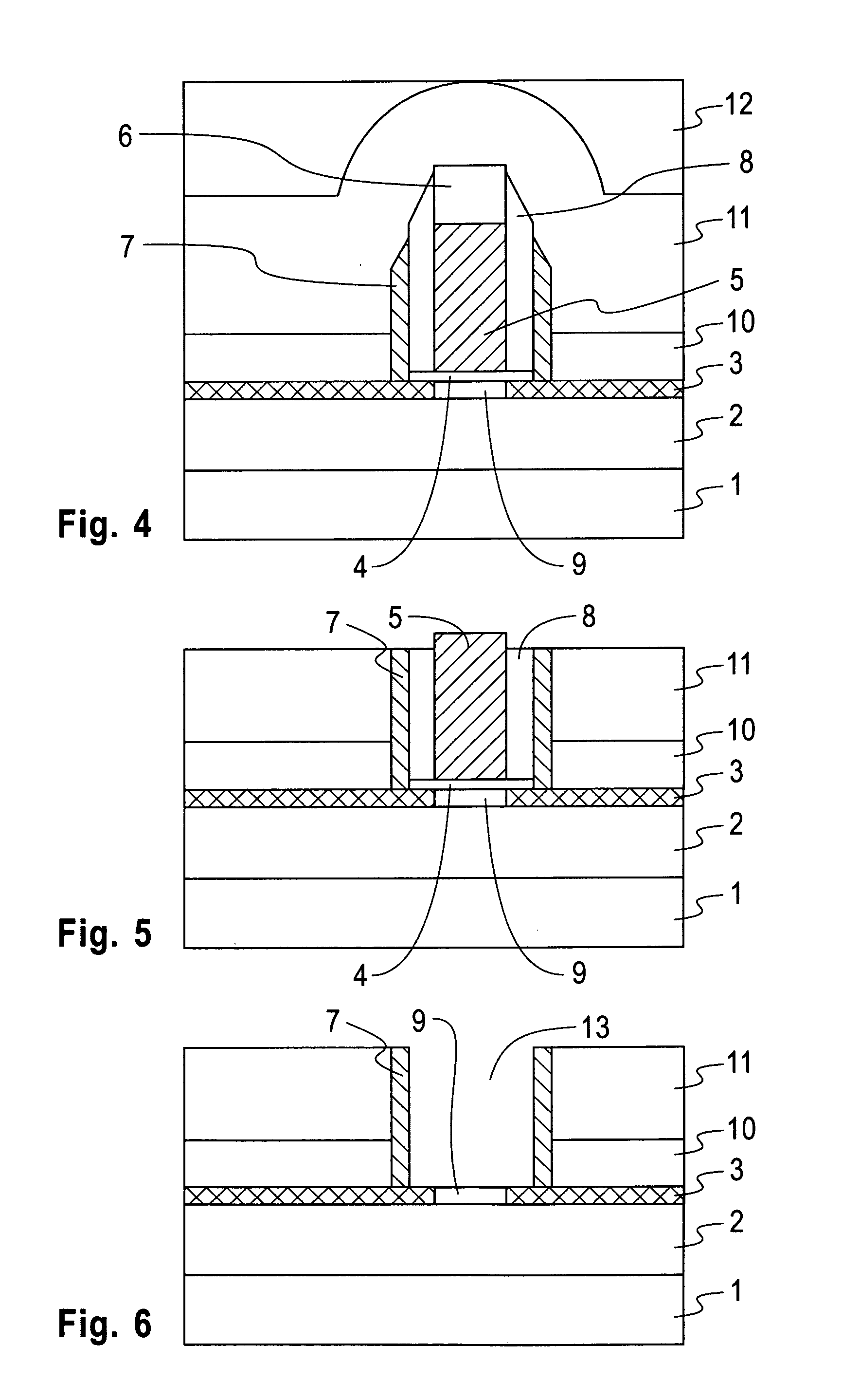
[0020] The present invention will now be described in more detail by referring to the drawings that accompany the present application. In the accompanying drawings, like reference numerals are used for describing like and corresponding elements.

[0021]FIG. 1 shows an initial stacked structure that comprises a substrate 1 having a bottom insulator 2, also referred to as buried oxide layer, located thereon. The initial stacked structure also includes a channel layer 3 on top of the bottom insulator 2, and an oxide layer 4, also referred to as pad protection layer, located atop the channel layer 3.

[0022] The structure shown in FIG. 1 can be manufactured from conventional materials with conventional processing steps that are well known in the art. For example, the substrate 1 may comprise any semiconducting material including, but not limited to: Si, Ge, SiGe, GaAs, InAs, InP and all other III / V semiconductor compounds, and may also be a layered substrate comprising different semicondu...


PUM


Abstract

A MOSFET is disclosed that comprises a channel between a source extension and a drain extension, a dielectric layer over the channel, a gate spacer structure formed on a peripheral portion of the dielectric layer, and a gate formed on a non-peripheral portion of the dielectric layer, with at least a lower portion of the gate surrounded by and in contact with an internal surface of the gate spacer structure, and the gate is substantially aligned at its bottom with the channel. One method of forming the MOSFET comprises forming the dielectric layer, the gate spacer structure and the gate contact inside a cavity that has been formed by removing a sacrificial gate and spacer structure.

Description

FIELD OF THE INVENTION [0001] The invention relates to a MOSFET device having a damascene gate with an internal spacer structure and a process of forming the device. BACKGROUND OF THE INVENTION [0002] In order to extend CMOS scaling, dielectrics of higher dielectric constant (Hi-K) are being investigated. For a given gate capacitance, hence charge in the channel, the Hi-K dielectric can be thicker, thus reducing tunneling leakage. To increase the gate capacitance even further, and to have a suitable work-function for thin-silicon implementation, a metal gate is desirable. These material options are frequently incompatible with conventional high-temperature front end of the line processing, so that replacement gate methods are being tried where the Hi-K dielectric and the metal are deposited in a groove formed by removing a dummy gate. [0003] As the gate length of a field effect transistor (FET) gets shorter, the Hi-K dielectric occupies an increasing fraction of the groove. The gate...

Claims


Application Information

Patent Timeline
Patent Type & Authority Applications(United States)
IPC IPC(8): H01L21/336H01L29/94
CPCH01L21/2652H01L21/28079H01L21/28088H01L21/28097H01L21/28114H01L21/28194H01L21/28229H01L29/42376H01L29/4908H01L29/495H01L29/4966H01L29/4975H01L29/513H01L29/517H01L29/665H01L29/66545H01L29/66553H01L29/6656H01L29/66628H01L29/66772H01L29/78654
Inventor GUHA, SUPRATIKHANAFI, HUSSEIN I.JAMMY, RAJARAOSOLOMON, PAUL M.
Owner GLOBALFOUNDRIES INC
Why Eureka
Try Eureka