Advanced quad flat no lead chip package having a protective layer to enhance surface mounting and manufacturing methods thereof

a technology of protective layer and chip package, which is applied in the direction of semiconductor devices, semiconductor/solid-state device details, electrical apparatus, etc., can solve the problems of not being able to meet most, or all, of the objectives of semiconductor chips, and the manufacturing process of such leadframes may not be scalable beyond two rows

Active Publication Date: 2009-09-17
ADVANCED SEMICON ENG INC
View PDF98 Cites 96 Cited by
  • Summary
  • Abstract
  • Description
  • Claims
  • Application Information

AI Technical Summary

Benefits of technology

[0002]The present invention relates generally to semiconductor chip packages. More particularly, this invention relates to an advanced Quad Flat No Lead (aQFN) chip package having a protective layer to enhance surface mounting and manufacturing methods thereof.

Problems solved by technology

Semiconductor chips have become progressively more complex, driven in large pan by the need for increasing processing power in a smaller chip size.
However, manufacturing processes for such leadframes may not be scalable beyond two rows of leads.
Current packaging solutions can meet some of these objectives but may not be able to meet most, or all, of these objectives.

Method used


Image

  • Advanced quad flat no lead chip package having a protective layer to enhance surface mounting and manufacturing methods thereof
  • Advanced quad flat no lead chip package having a protective layer to enhance surface mounting and manufacturing methods thereof
  • Advanced quad flat no lead chip package having a protective layer to enhance surface mounting and manufacturing methods thereof

Examples


Embodiment Construction

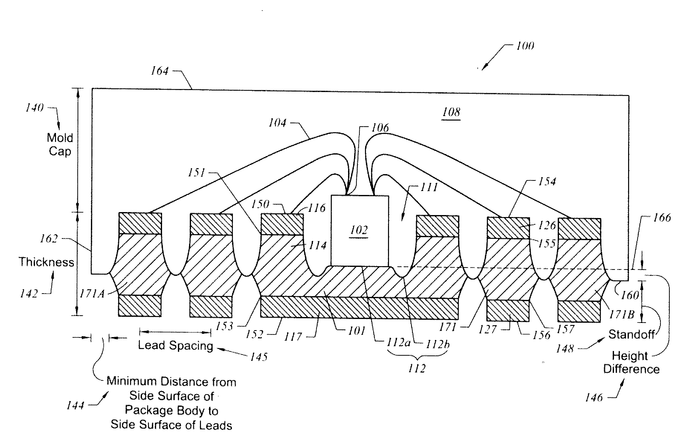
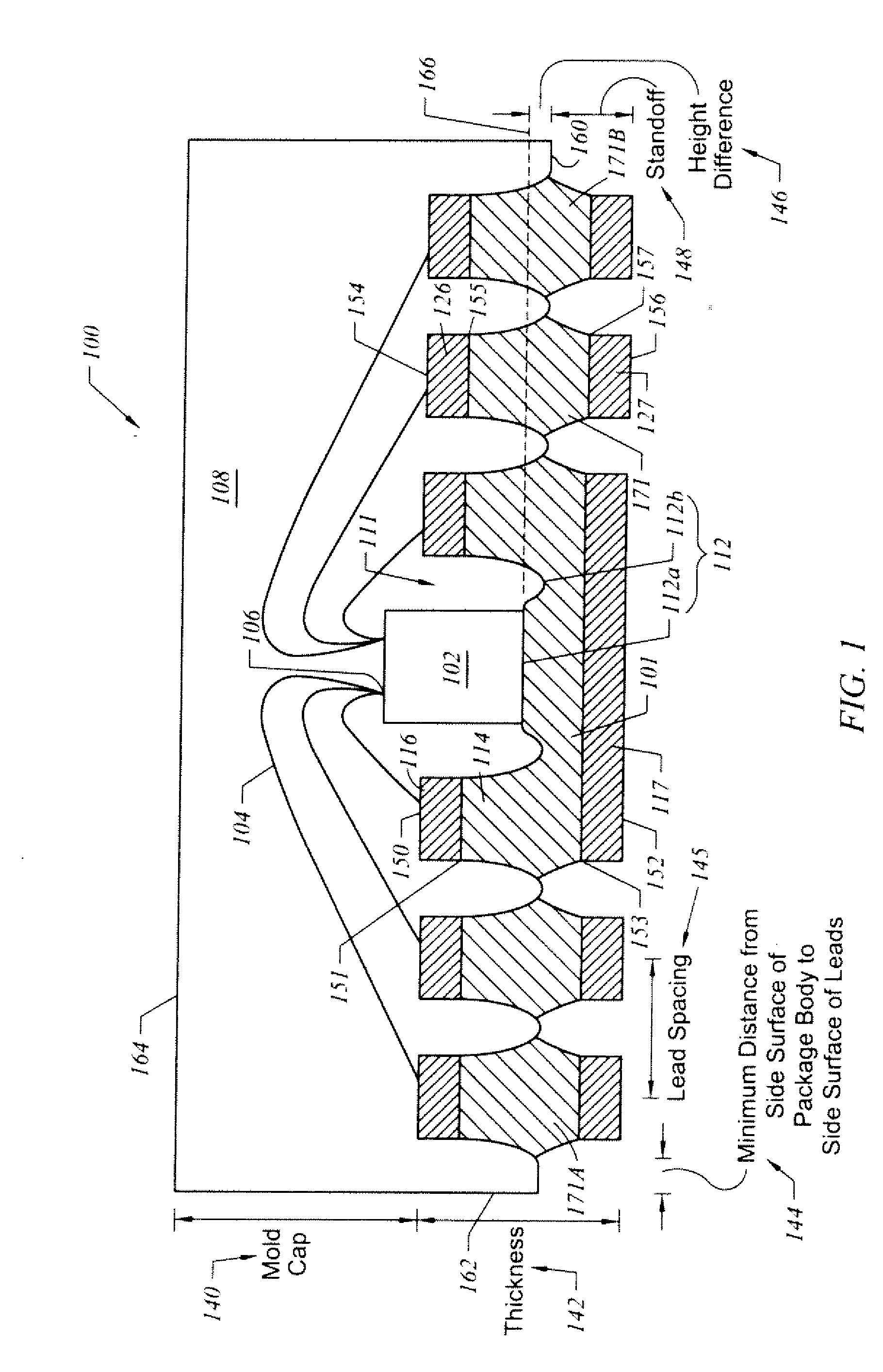
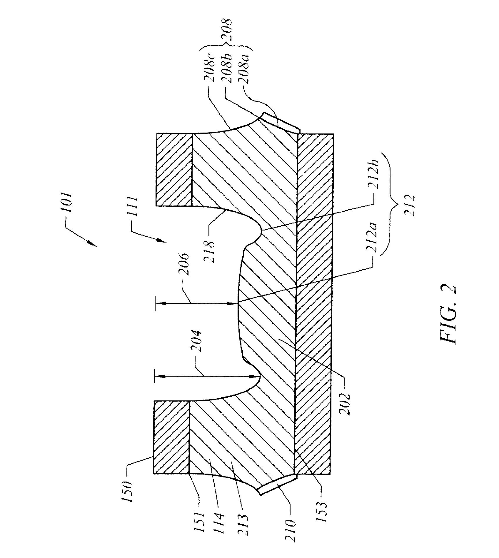
[0020]FIG. 1 illustrates a cross-sectional view of a semiconductor package 100, in accordance with one embodiment of the present invention. The package 100 includes a die pad 101 with a peripheral edge region 114 that defines a cavity 111 with a cavity bottom 112. The peripheral edge region 114 may completely surround the cavity 111, but also can partially surround the cavity 111 for certain implementations. The cavity bottom 112 includes a central portion 112a. The cavity bottom 112 may also include a recess 112b around the central portion 112a. The central portion 112a may be approximately centrally located within the cavity bottom 112, but need not be if, for example, the recess 112b is of non-uniform width. The recess 112b may completely surround the central portion 112a, but also can partially surround the central portion 12a for certain implementations. A chip 102 is attached to the cavity bottom 112 by an adhesive layer (not shown). The adhesive layer may be a conductive or a...


PUM


Abstract

A semiconductor package and related methods are described. In one embodiment, the package includes a die pad, multiple leads, a chip, a package body, and a protective layer. The die pad includes an upper sloped portion, a lower sloped portion, and a peripheral edge region defining a cavity with a cavity bottom. Each lead includes an upper sloped portion and a lower sloped portion. The chip is disposed on the cavity bottom and is coupled to the leads. The package body is formed over the chip and the leads, substantially fills the cavity, and substantially covers the upper sloped portions of the die pad and the leads. The lower sloped portions of the die pad and the leads at least partially extend outwardly from a lower surface of the package body. The protective layer substantially covers the lower sloped portion and the lower surface of at least one lead.

Description

CROSS-REFERENCE TO RELATED APPLICATION[0001]The present application claims the benefit of the following commonly owned U.S. provisional patent application, which is incorporated herein by reference in its entirety: U.S. Provisional Patent Application No. 61 / 036,470, Attorney Docket No. ASEG-0001 / 00US, entitled “Chip Package Structure and Manufacturing Methods Thereof,” filed on Mar. 14, 2008.FIELD OF THE INVENTION[0002]The present invention relates generally to semiconductor chip packages. More particularly, this invention relates to an advanced Quad Flat No Lead (aQFN) chip package having a protective layer to enhance surface mounting and manufacturing methods thereof.BACKGROUND OF THE INVENTION[0003]Semiconductor chips have become progressively more complex, driven in large pan by the need for increasing processing power in a smaller chip size. In response, packaging technologies have evolved, for example, to enable an increased lead density, which can reduce the footprint area of...

Claims


Application Information

Patent Timeline
Patent Type & Authority Applications(United States)
IPC IPC(8): H01L23/495H01L21/60
CPCH01L21/4832H01L23/3107H01L2924/07802H01L2224/73265H01L2224/32145H01L2924/12041H01L2224/32245H01L2924/01087H01L24/48H01L2924/30105H01L2924/19041H01L2924/01082H01L2924/01079H01L2924/01078H01L2924/01075H01L2924/01046H01L2924/01033H01L2924/01029H01L2924/01013H01L2924/01002H01L2224/97H01L2224/92247H01L2224/48247H01L2224/48091H01L2224/32257H01L23/49548H01L23/49582H01L24/97H01L2224/85H01L2924/00014H01L2924/00012H01L2924/00H01L24/73H01L2924/181H01L2224/49433H01L2224/45099H01L2224/45015H01L2924/207
Inventor CHEN, CHIEN-WENTSENG, AN-SHIHLAI, YI-SHAOCHANG, HSIAO-CHUANTSAI, TSUNG-YUEH
Owner ADVANCED SEMICON ENG INC
Why Eureka
Try Eureka