Requirement management device, requirement management method, computer product
- Summary
- Abstract
- Description
- Claims
- Application Information
AI Technical Summary
Benefits of technology
Problems solved by technology
Method used
Image

Examples
example
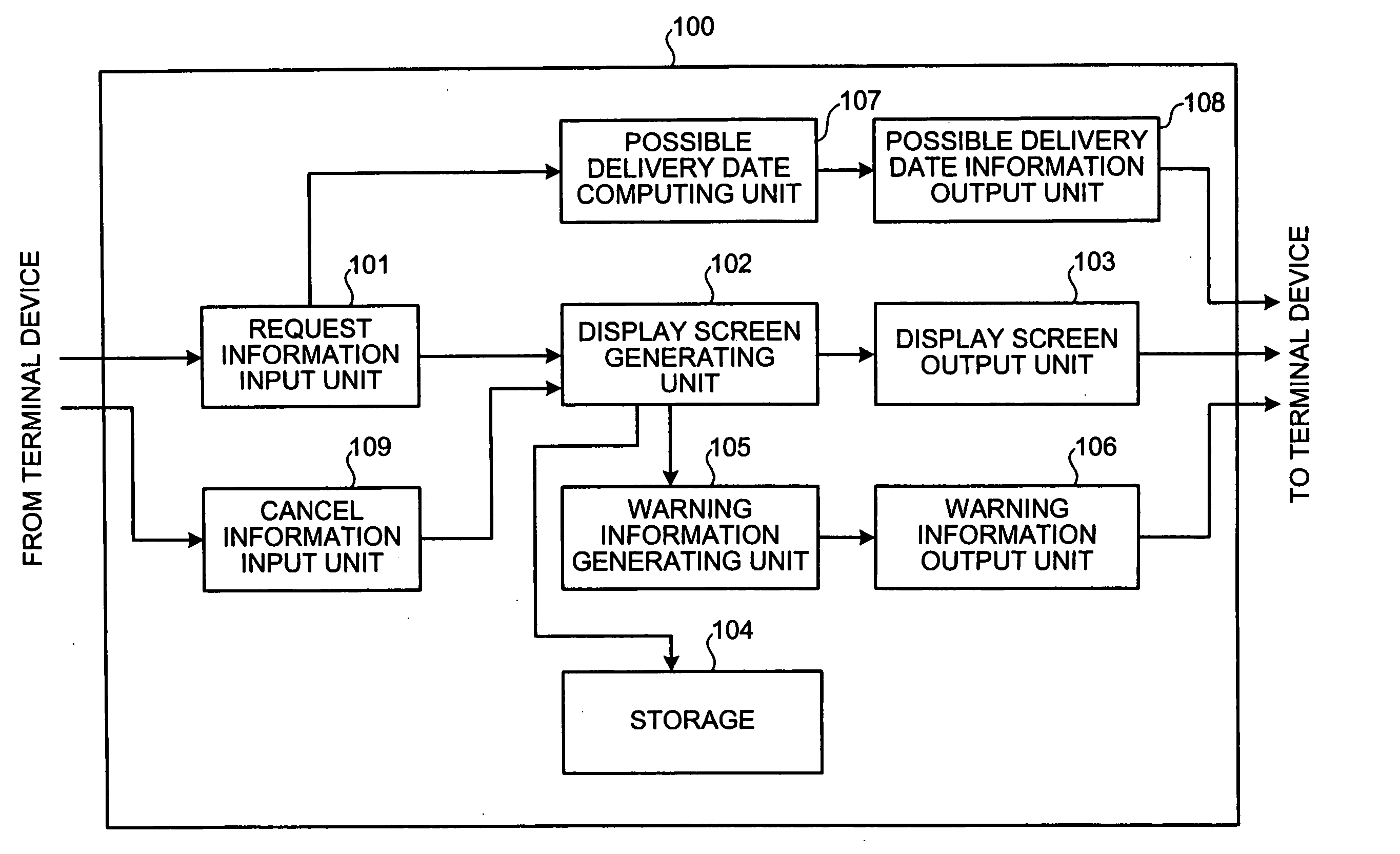
[0074]FIG. 4 is a detailed diagram to explain an example of manufacturing process of a semiconductor product according to the present example of this invention. The manufacturing process of a semiconductor product shown in FIG. 4, as one example, consists of a “capacity adjustment” step 401, a “diffusion” step 402 of ca. two weeks, a “wiring” step 403 of ca. two weeks, a “wafer test” step 404 of 0.5 week, a “wafer visual test” step 405 of ca. 0.5 week (that is, about one week of the “wafer test” step 404 and the “wafer visual test” step 405), an “assembly” step 406 of ca. one week, and a “final test” step 407 of ca. one week. Accordingly, it takes about seven weeks from preparation (start of the “diffusion” step 402) to completion of a finished product (end of the “final test” step 407).
[0075] A point of preparation instruction at the factory differs depending on requirement ranks. Each point is determined at the time when the “diffusion” step 402 starts, the time when “wiring” ste...
PUM
 Abstract
Description
Claims
Application Information
 - R&D Engineer
- R&D Manager
- IP Professional
- Industry Leading Data Capabilities
- Powerful AI technology
- Patent DNA Extraction
Browse by: Latest US Patents, China's latest patents, Technical Efficacy Thesaurus, Application Domain, Technology Topic.
© 2024 PatSnap. All rights reserved.Legal|Privacy policy|Modern Slavery Act Transparency Statement|Sitemap