Optical scanning device and image forming apparatus

Inactive Publication Date: 2008-08-14
RICOH KK
View PDF36 Cites 59 Cited by
  • Summary
  • Abstract
  • Description
  • Claims
  • Application Information

AI Technical Summary

Benefits of technology

[0014]It is an object of the present invention to at least

Problems solved by technology

This poses problems regarding durability of a shaft, heating due to windage loss, noise, and others, thereby limiting high-speed scanning.
Therefore, an fθ lens used for a present write optical system is used for a scanning image-formation optical system, the scanning speed is low in a peripheral image height, and therefore the scanning speed on the surface to be scanned is not uniform.
If the uniformity of the scanning speed is poor, image distortion and other disadvantages may occur near a main scanning direction, thereby causing deterioration in image quality.
Moreover, although Japanese Patent Application Laid-Open No. 2004-279947 also discloses an electrical correction of the speed uniformity, if a difference caused by this correction from the original is large, dots become sparse or concentrated stepwise, thereby changing density and causing an image deterioration.
For this reason, the amount of electrical correction has a limitation.
When a vibration mirror and an fθ lens that vibrate in a sine wav

Method used


Image

  • Optical scanning device and image forming apparatus
  • Optical scanning device and image forming apparatus
  • Optical scanning device and image forming apparatus

Examples


second embodiment

[0123]In the first embodiment explained above, the stepping motor in FIG. 6 is used as a unit of driving the coupling lens in the optical-axis direction. Alternatively, as a light-source unit 700 depicted in FIGS. 16A and 16B, an actuator, such as a voice coil, may be used.

[0124]In FIGS. 16A and 16B, a semiconductor laser 701 as a light source fits in a through hole 703 of a holder member 702 by pressure from a side opposite to a surface that abuts on a housing not shown coaxially with the through hole 703. On the surface side that abuts on the housing of the holder member 702, a cylindrical portion 709 is integrally formed coaxially with the through hole 703. Along an internal circle of the cylindrical portion, an electromagnetic coil 704 wounded in a cylindrical shape is inserted. A reference numeral 706 represents a coupling lens, such as a collimator lens. The coupling lens 706 forms a first image-formation optical system that converts the light beam from the light-emitting sour...

third embodiment

[0129]Next, a third embodiment is explained in which a variable-focus lens as depicted in FIG. 23 is used as a coupling lens to make the beam-spot diameters on the surface of the photosensitive member uniform. A configuration example of a light-source unit using this variable-focus lens as a coupling lens is depicted in FIG. 24.

[0130]This light-source unit includes a light source 21 and a variable-focus lens unit 13. The variable-focus lens unit 13 includes a variable-focus lens 14 and a fixed object lens 15.

[0131]FIG. 23 depicts a detailed drawing of the variable-focus lens unit 13. The variable-focus lens 14 of this variable-focus lens unit 13 has the following configuration so as to have a thin thickness with respect to a focal length of the fixed object lens 15.

[0132]With respect to an annular silicon spacer 24, a thin-film glass diaphragm 25 as a translucent elastic film is jointed through positive-polarity junction. On the glass diaphragm 25, a piezoelectric element 26 made of...

fourth embodiment

[0135]Next, a fourth embodiment is explained by using FIG. 14, in which a depth enlarging unit is used, instead of moving the coupling lens in an optical-axis direction for correction in field curvature, to make the beam-spot diameters uniform on the surface of the photosensitive member.

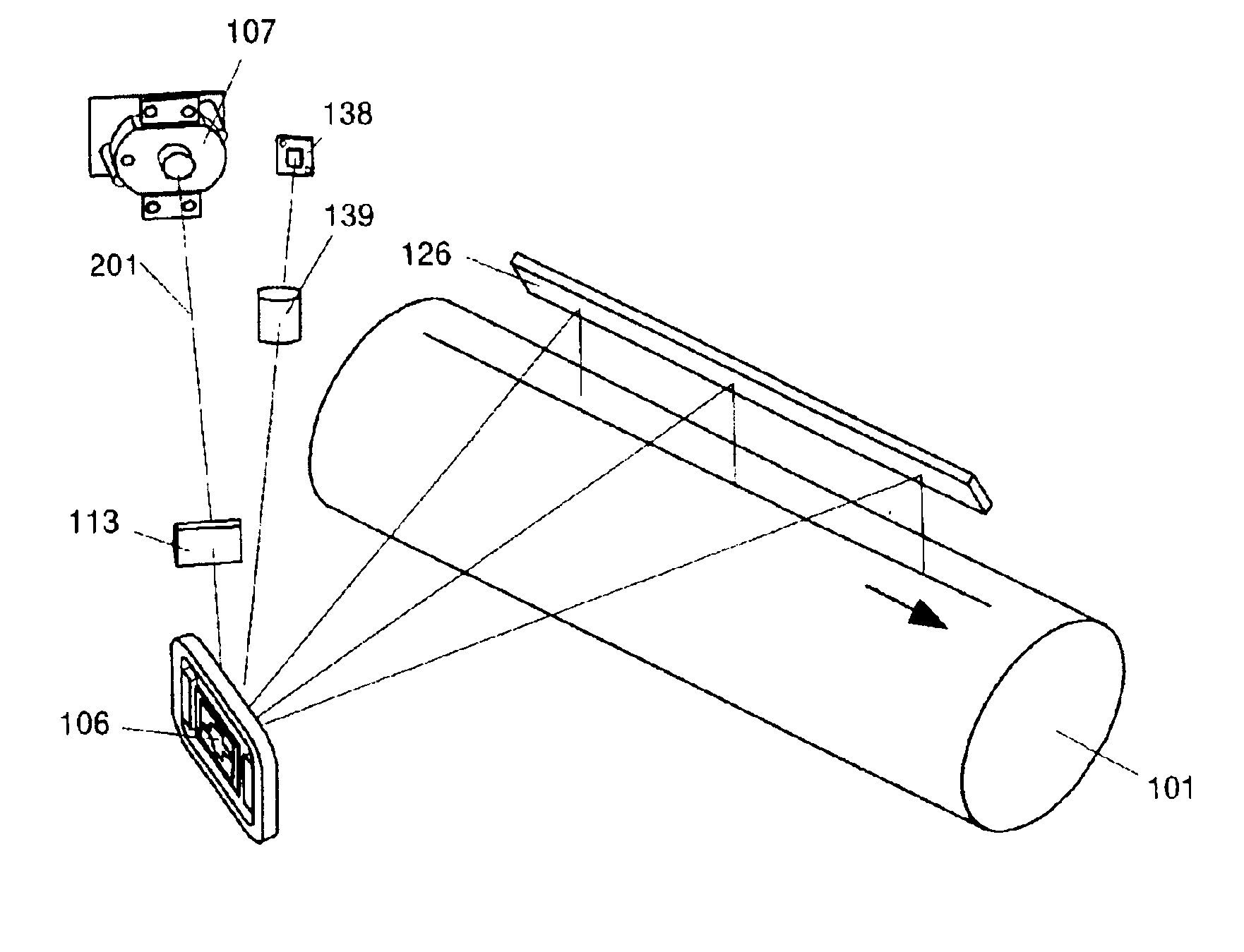
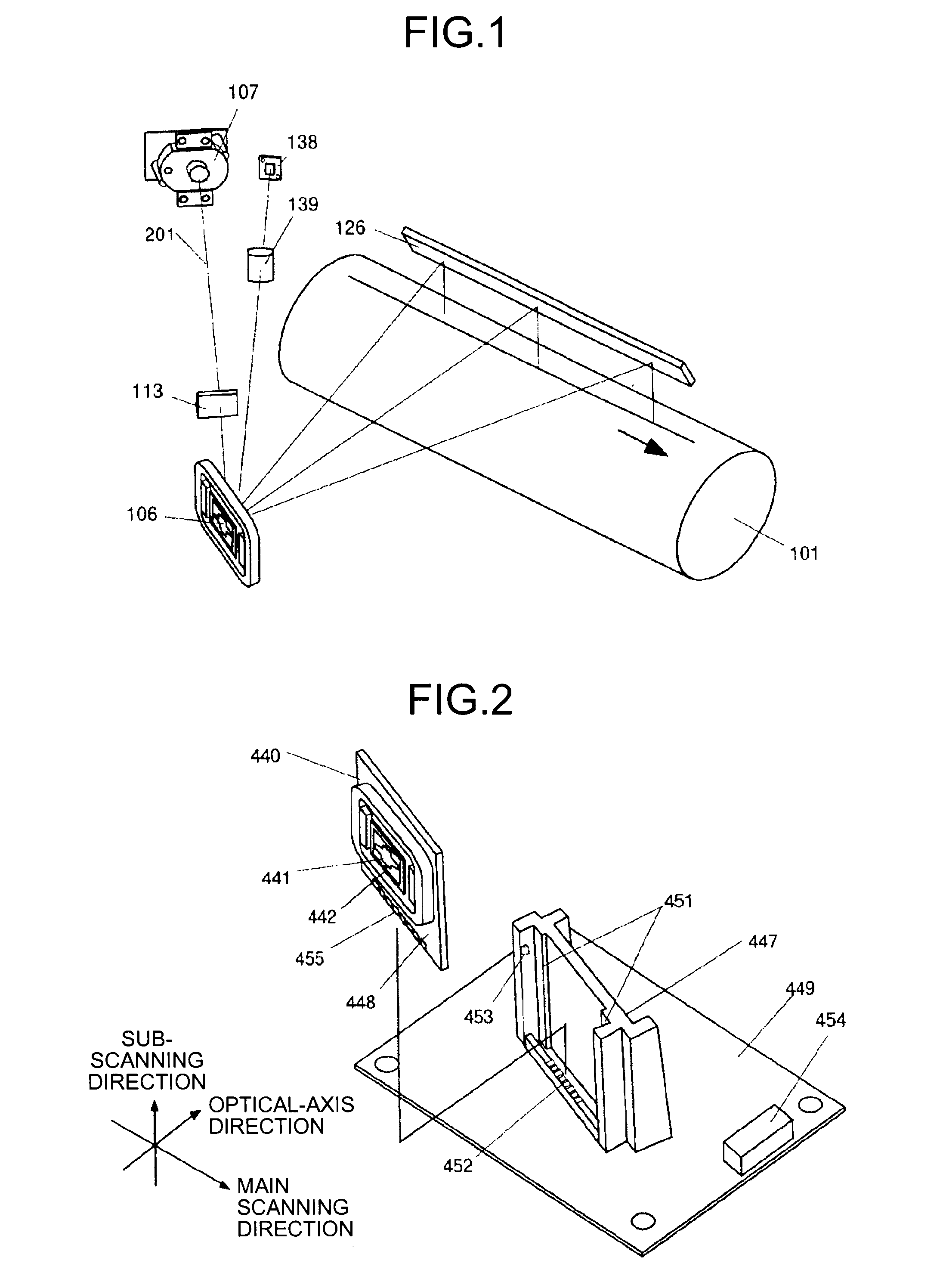
[0136]The basic configuration of the optical scanning device of FIG. 14 is similar to the configuration of FIG. 1 explained in the first embodiment, but is different therefrom in that a depth enlarging unit 301 is disposed between the light-source unit 107 and the vibration mirror 106. Also, the optical scanning device according to the present embodiment does not include a unit of moving the coupling lens in an optical-axis direction, which is as depicted in FIG. 6 and disposed in the first embodiment.

[0137]The depth enlarging unit 301 is provided with a phase-type optical element that increases a side-lobe peak intensity, for example. With this, a depth margin is enlarged. A large ratio of enlarging...


PUM


Abstract

An optical scanning device includes, in an effective scanning area in the target surface, a mechanism that causes a scanning speed at each scanning position with respect to a scanning speed at an approximately center in the effective scanning area to be within a range under a predetermined condition.

Description

CROSS-REFERENCE TO RELATED APPLICATIONS[0001]The present application claims priority to and incorporates by reference the entire contents of Japanese priority document 2007-031947 filed in Japan on Feb. 13, 2007.BACKGROUND OF THE INVENTION[0002]1. Field of the Invention[0003]The present invention relates to optical scanning devices applicable to optical scanning devices for use in an electrophotographic image forming apparatus.[0004]2. Description of the Related Art[0005]In optical scanning apparatuses, a polygon mirror or a galvanometer mirror is used as a deflector for scanning with an optical beam. To achieve higher-resolution images and higher-speed printing, the rotation speed of the deflector has to be further increased. This poses problems regarding durability of a shaft, heating due to windage loss, noise, and others, thereby limiting high-speed scanning.[0006]To get around these problems, deflecting devices using silicon micromachining has been studied in recent years. For ...

Claims


Application Information

Patent Timeline
IPC IPC(8): G02B26/10
CPCG02B26/105B41J2/471G02B3/14
Inventor NAKAMURA, TADASHINAKAJIMA, TOMOHIROIMAI, SHIGEAKI
Owner RICOH KK
Why Eureka
Try Eureka