Thin film transistor, method of manufacturing the same, display apparatus having the same and method of manufacturing the display apparatus

a technology of thin film transistors and display devices, which is applied in the direction of non-linear optics, identification means, instruments, etc., can solve the problems of undesirable irregularities on low-resistance metals, delayed or distorted signals applied to signal lines, undesirable after-images on liquid crystal display devices, etc., and achieve the effect of improving the display quality thereo

Active Publication Date: 2006-06-08
SAMSUNG DISPLAY CO LTD
View PDF6 Cites 13 Cited by
  • Summary
  • Abstract
  • Description
  • Claims
  • Application Information

AI Technical Summary

Benefits of technology

[0023] According to the above, the barrier pattern and the conductive adhesive pattern are formed by the dry etching process, so that the display a

Problems solved by technology

As a result of the signal lines being longer, signals applied to the signal lines are delayed or distorted.
However, an undesirable irregularity forms o

Method used


Image

  • Thin film transistor, method of manufacturing the same, display apparatus having the same and method of manufacturing the display apparatus
  • Thin film transistor, method of manufacturing the same, display apparatus having the same and method of manufacturing the display apparatus
  • Thin film transistor, method of manufacturing the same, display apparatus having the same and method of manufacturing the display apparatus

Examples


Embodiment Construction

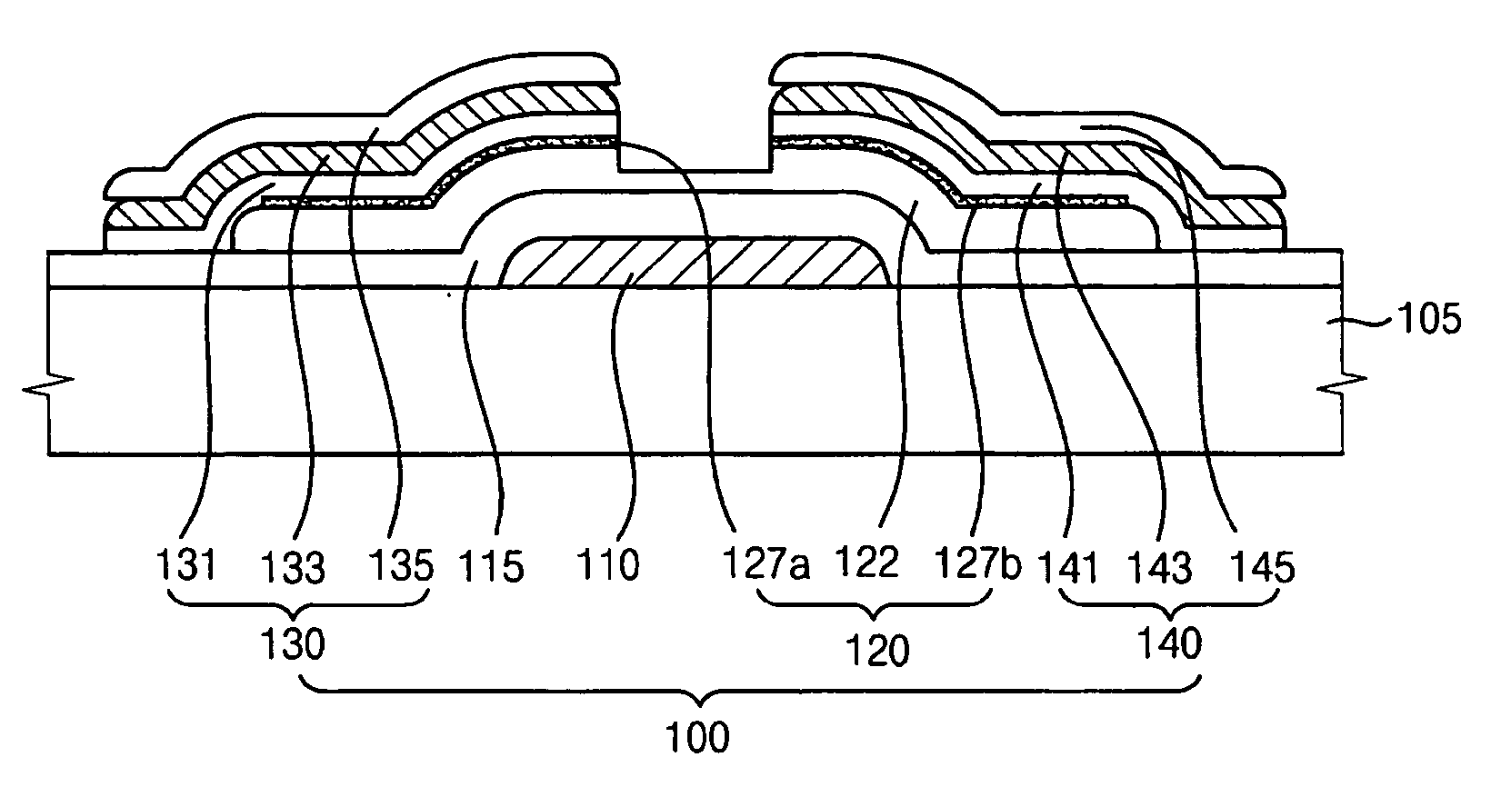
[0033] It will be understood that when an element or layer is referred to as being “on”, “connected to” or “coupled to” another element or layer, it can be directly on, connected or coupled to the other element or layer or intervening elements or layers may be present. In contrast, when an element is referred to as being “directly on,”“directly connected to” or “directly coupled to” another element or layer, there are no intervening elements or layers present. Like numbers refer to like elements throughout. As used herein, the term “and / or” includes any and all combinations of one or more of the associated listed items.

[0034] It will be understood that, although the terms first, second, etc. may be used herein to describe various elements, components, regions, layers and / or sections, these elements, components, regions, layers and / or sections should not be limited by these terms. These terms are only used to distinguish one element, component, region, layer or section from another ...


PUM


Abstract

A thin film transistor includes a gate electrode on a substrate, a gate insulating layer on the substrate, a channel pattern, a source electrode and a drain electrode. The channel pattern includes a semiconductor pattern formed on the gate electrode and overlaying the gate electrode as well as first and second conductive adhesive patterns formed on the semiconductor pattern and spaced apart from each other. The source electrode includes a first barrier pattern, a source pattern and a first capping pattern sequentially formed on the first conductive adhesive pattern. The drain electrode includes a second barrier pattern, a drain pattern and a second capping pattern sequentially formed on the second conductive adhesive pattern. Etched portions of the first and second conductive adhesive patterns have a substantially vertical profile to prevent the exposure of the source and drain electrodes, thereby improving the characteristics of the thin film transistor.

Description

CROSS-REFERENCE TO RELATED APPLICATIONS [0001] This application relies for priority upon Korean Patent Application No. 2004-103221 filed on Dec. 8, 2004, the content of which is herein incorporated by reference in its entirety. BACKGROUND OF THE INVENTION [0002] 1. Field of the Invention [0003] The present invention relates to a thin film transistor, a method of manufacturing the same, a display apparatus having the same and a method of manufacturing the display apparatus. More particularly, the present invention relates to a thin film transistor for an array substrate of a display apparatus, a method of manufacturing the thin film transistor, a display apparatus having the thin film transistor and a method of manufacturing the display apparatus. [0004] 2. Description of the Related Art [0005] In general, a liquid crystal display apparatus includes an array substrate and a color filter substrate. The array substrate includes a thin film transistor acting as a switching device and a ...

Claims


Application Information

Patent Timeline
IPC IPC(8): H01L29/04G02F1/1368G09F9/30H01L21/28H01L21/3205H01L21/336H01L21/768H01L23/532H01L29/417H01L29/423H01L29/49H01L29/786
CPCG02F1/1368H01L27/12H01L27/124H01L29/66765H01L29/458G02F1/136
Inventor KIM, SANG-GABKIM, SHI--YULPARK, HONG-SICKCHOE, HEE-HWANCHIN, HONG-KEEOH, MIN-SEOK
Owner SAMSUNG DISPLAY CO LTD
Why Eureka
Try Eureka