Multi-chip package structure

a technology of multi-chips and packaging, applied in the direction of semiconductor devices, semiconductor/solid-state device details, electrical devices, etc., can solve the problems of increasing manufacturing costs and prolonging research time, and achieve the effect of avoiding the shortcoming of large area

Inactive Publication Date: 2006-06-29
ADVANCED SEMICON ENG INC
View PDF18 Cites 74 Cited by
  • Summary
  • Abstract
  • Description
  • Claims
  • Application Information

AI Technical Summary

Benefits of technology

[0011] One objective of the present invention is to provide a package structure having a sub-package therein. The package structure of the present invention is formed by stacking so as to avoid the shortcoming of large area caused by parallel arrangement of a plurality of conventional package structures.
[0012] Another objective of the present invention is to provide a package structure having a sub-package therein. The sub-package is a package that has been tested, and is integrated into the package structure of the present invention as a Known-Good Die (KGD). The manufacture cost of the package structure of the present invention is reduced because package test is cheaper and easier than Known-Good Die test.
[0013] Another objective of the present invention is to provide a package structure having a sub-package therein. The package structure of the present invention has at least two chips; therefore, there is no need to redesign the signal-transmitting path between the chips.

Problems solved by technology

Because different memory chips have different sizes and different amounts of I / O pins, it is necessary to redesign signal-transmitting path when the microprocessor chip is integrated with different memory chips, which increases the manufacture cost and extends the research time.

Method used


Image

  • Multi-chip package structure
  • Multi-chip package structure
  • Multi-chip package structure

Examples


first embodiment

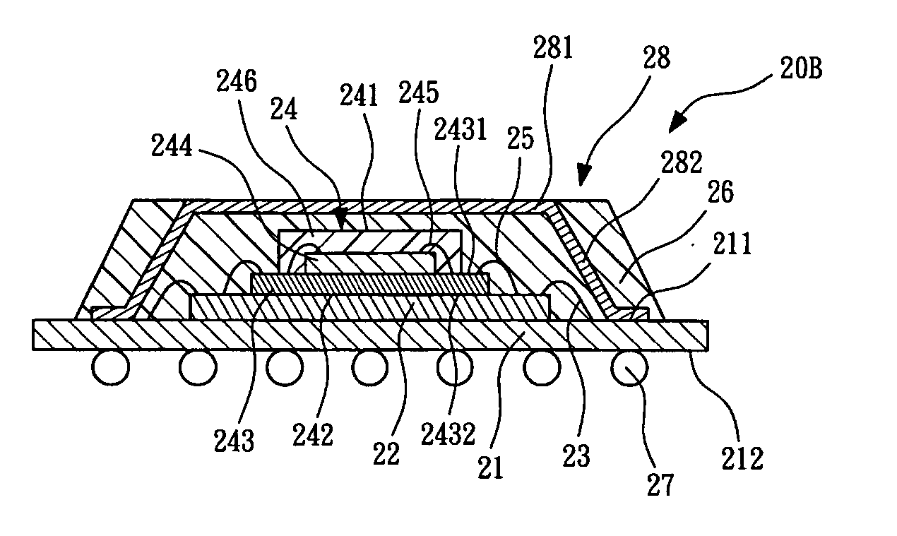
[0037]FIG. 3 shows a cross sectional view of a multi-chip package structure according to the present invention. The multi-chip package structure 20A of the embodiment comprises a first substrate 21, a first chip 22, a plurality of first wires 23, a sub-package 24, a plurality of third wires 25, a first molding compound 26 and a plurality of solder balls 27.

[0038] The first substrate 21 has a top surface 211 and a bottom surface 212. The first chip 22 is attached to the top surface 211 of the first substrate 21 and is electrically connected to the first substrate 21 by utilizing the first wires 23. It is to be noted that if the first chip 22 is attached to the first substrate 21 by flip-chip, there is no need to dispose the first wires 23.

[0039] The sub-package 24 has a top surface 241 and a bottom surface 242. The bottom surface 242 of the sub-package 24 is attached to the first chip 22 by utilizing adhesive glue. The sub-package 24 includes a second substrate 243, a second chip 24...

fourth embodiment

[0046]FIG. 6 shows a cross sectional view of a multi-chip package structure according to the present invention. The multi-chip package structure 30A of the embodiment comprises a first substrate 31, a first chip 32, a plurality of first wires 33, a sub-package 34, a plurality of third wires 35, a first molding compound 36, a plurality of solder balls 37, a third chip 38 and a plurality of fourth wires 39.

[0047] The first substrate 31 has a top surface 311 and a bottom surface 312. The first chip 32 is attached to the top surface 311 of the first substrate 31 and is electrically connected to the first substrate 31 by utilizing the first wires 33. It is to be noted that if the first chip 32 is attached to the first substrate 31 by flip-chip, there is no need to dispose the first wires 33.

[0048] The sub-package 34 has a top surface 341 and a bottom surface 342. The bottom surface 342 of the sub-package 34 is attached to the first chip 32 by utilizing adhesive glue. The sub-package 34 ...

eighth embodiment

[0066]FIG. 15 shows a cross sectional view of a multi-chip package structure according to the present invention. The multi-chip package structure 60 of the embodiment comprises a first sub-package 61, a second sub-package 62, a third substrate 63, a third molding compound 64, a plurality of third wires 65, a plurality of fourth wires 66 and a plurality of solder balls 67.

[0067] The third substrate 63 has a top surface 631 and a bottom surface 632. The third molding compound 64 is used for encapsulating the first sub-package 61, the second sub-package 62 and the top surface 631 of the third substrate 63. The third wires 65 electrically connect the third substrate 63 and the first sub-package 61. The fourth wires 66 electrically connect the third substrate 63 and the second sub-package 62. The solder balls 67 are formed on the bottom surface 632 of the third substrate 63.

[0068] The first sub-package 61 has a top surface 611 and a bottom surface 612, and further comprises a first subs...


PUM


Abstract

The present invention relates to a multi-chip package structure, comprising a first substrate, a first chip, a sub-package and a first molding compound. The first chip is attached to the first substrate. The first molding compound encapsulates the first chip, the sub-package and the top surface of the first substrate. The bottom surface of the sub-package is attached to the first chip. The sub-package comprises a second substrate, a second chip and a second molding compound. The second substrate has a top surface and a bottom surface, and is electrically connected to the first chip. The second chip is attached to the top surface of the second substrate to which the second chip is electrically connected. The second molding compound encapsulates the second chip and part of the top surface of the second substrate. Whereby, the relative large area caused by the parallel arrangement of a plurality of conventional package structures can be reduced, and there is no need to redesign signal-transmitting path.

Description

CROSS-REFERENCE TO RELATED APPLICATION [0001] This is a continuation-in-part of U.S. application Ser. No. 11 / 026,763, filed Dec. 31, 2004, entitled “Multi-Chip Package Structure.”BACKGROUND OF THE INVENTION [0002] 1. Field of the Invention [0003] The present invention relates to a multi-chip package structure, particularly to a multi-chip package structure having a sub-package. [0004] 2. Description of the Related Art [0005] The requirement of high density, high performance and precise cost control of an electronic product speeds up the developments of System On a Chip (SOC) and System In a Package (SIP). The mostly used package technique is Multi-Chip Module (MCM), which integrates the chips having different functions, such as microprocessors, memories, logic elements, optical ICs and capacitors, and replaces the prior art of disposing individual packages on one circuit board. [0006]FIGS. 1 and 2 show the perspective and cross-sectional views of a conventional Multi-Chip Module pac...

Claims


Application Information

Patent Timeline
Patent Type & Authority Applications(United States)
IPC IPC(8): H01L23/02
CPCH01L23/3128H01L23/3135H01L23/4334H01L25/0657H01L25/105H01L2224/32145H01L2224/48091H01L2224/48145H01L2224/48227H01L2225/06506H01L2225/0651H01L2225/06572H01L2924/15311H01L2924/16152H01L2924/19041H01L2924/00014H01L24/48H01L25/03H01L2225/1023H01L2225/1052H01L2924/19107H01L2924/181H01L2924/18165H01L2924/00012H01L2224/45099H01L2224/45015H01L2924/207
Inventor TAO, SUTSAI, YU-FANG
Owner ADVANCED SEMICON ENG INC
Why Eureka
Try Eureka