Plasma display panel and manufacturing method thereof
a technology of display panel and plasma, which is applied in the direction of gas discharge electrodes, gas discharge vessels/containers, gas-filled discharge tubes, etc., can solve the problems of poor adhesive strength of front substrates with substrates, short black layer patterns, and partial peeling phenomenon, so as to reduce failure rate and enhance production yield
- Summary
- Abstract
- Description
- Claims
- Application Information
AI Technical Summary
Benefits of technology
Problems solved by technology
Method used
Image

Examples
Embodiment Construction
[0032] Embodiments of the present invention will be described in a more detailed manner with reference to the drawings.
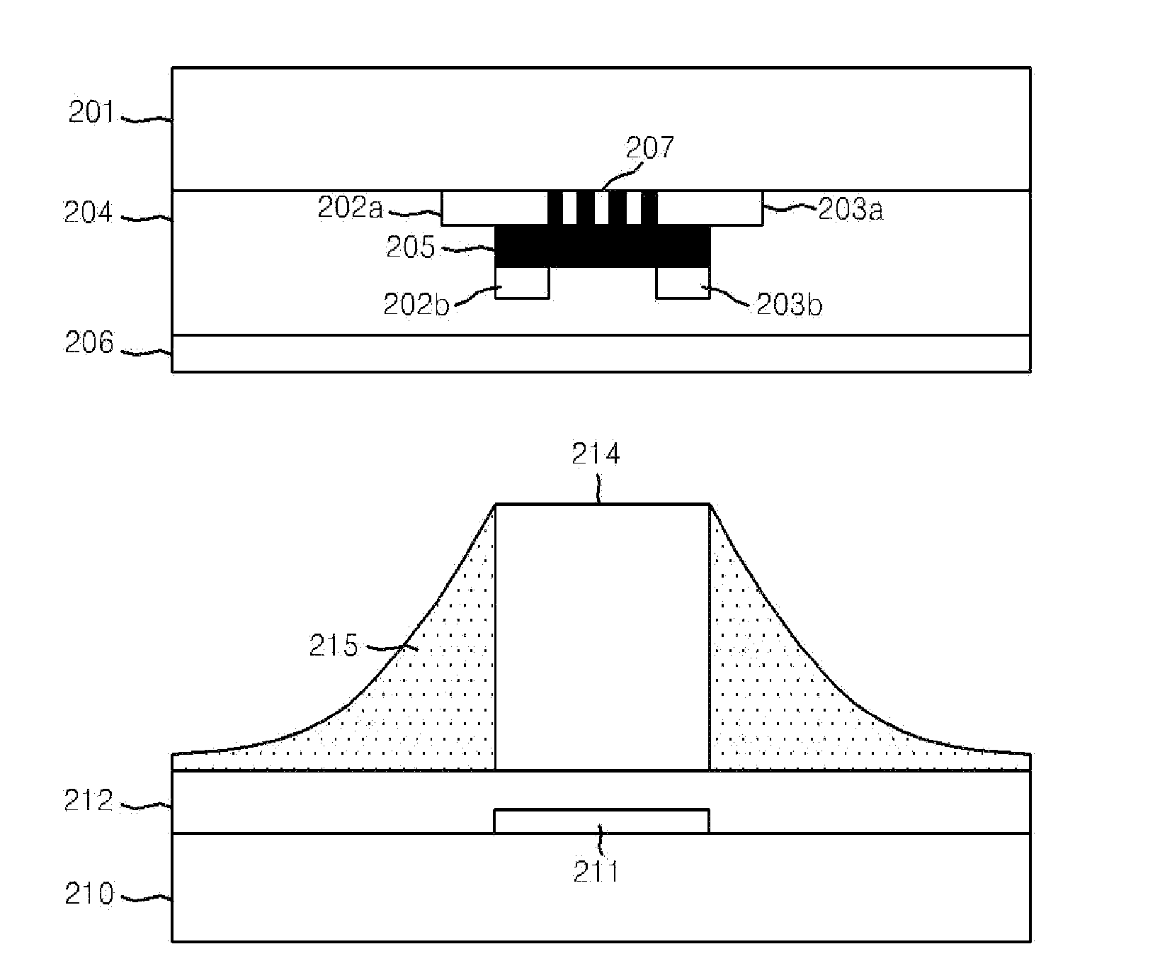
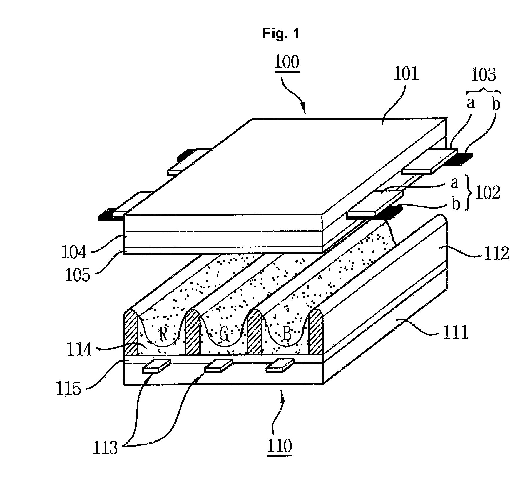
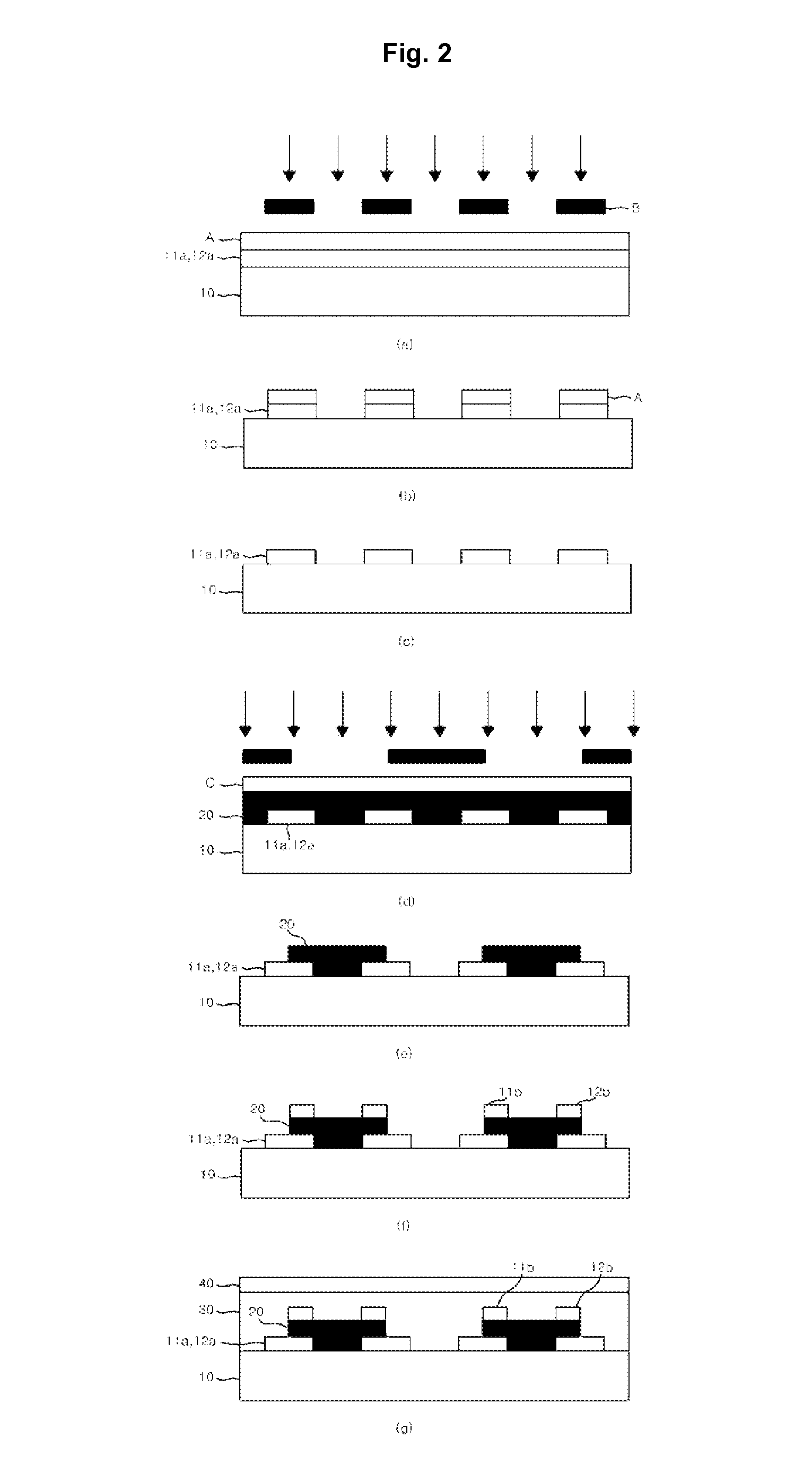
[0033] A plasma display panel according to an embodiment of the present invention comprises a front glass substrate, a transparent electrode formed on the front glass substrate in a discharge region, an adhesive agent formed at least on a portion of the front glass substrate in a non-discharge region and a black layer formed on the adhesive agent in the non-discharge region.
[0034] The black layer is further formed on some portion of the transparent electrode
[0035] The plasma display panel further comprises a bus electrode formed on the black layer.
[0036] The adhesive agent and the transparent electrode are formed of an ITO material.
[0037] The adhesive agent has a dot pattern.
[0038] The dot pattern comprises one or more dots.
[0039] The adhesive agent has a line pattern.
[0040] The line pattern comprises one or more lines.
[0041] The transparent electrode compr...
PUM
 Abstract
Description
Claims
Application Information
 - R&D Engineer
- R&D Manager
- IP Professional
- Industry Leading Data Capabilities
- Powerful AI technology
- Patent DNA Extraction
Browse by: Latest US Patents, China's latest patents, Technical Efficacy Thesaurus, Application Domain, Technology Topic.
© 2024 PatSnap. All rights reserved.Legal|Privacy policy|Modern Slavery Act Transparency Statement|Sitemap