Ocb mode liquid crystal display and a driving method of the same

a liquid crystal display and driving method technology, applied in the field of ocb, can solve the problems of low contrast ratio and high luminance in the black state and achieve the effect of improving the contrast ratio of the ocb mode lcd

Inactive Publication Date: 2006-06-29
SAMSUNG DISPLAY CO LTD
View PDF3 Cites 22 Cited by
  • Summary
  • Abstract
  • Description
  • Claims
  • Application Information

AI Technical Summary

Problems solved by technology

However, an OCB mode LCD has a problem of low contrast ratio.
It is because the OCB mode LCD gives relatively high luminance in a black state in comparison with other mode LCDs, and the high luminance in the black state is caused by the difficulty in complete compensation of the wavelength dispersion of LCD using compensation films.

Method used


Image

  • Ocb mode liquid crystal display and a driving method of the same
  • Ocb mode liquid crystal display and a driving method of the same
  • Ocb mode liquid crystal display and a driving method of the same

Examples


first embodiment

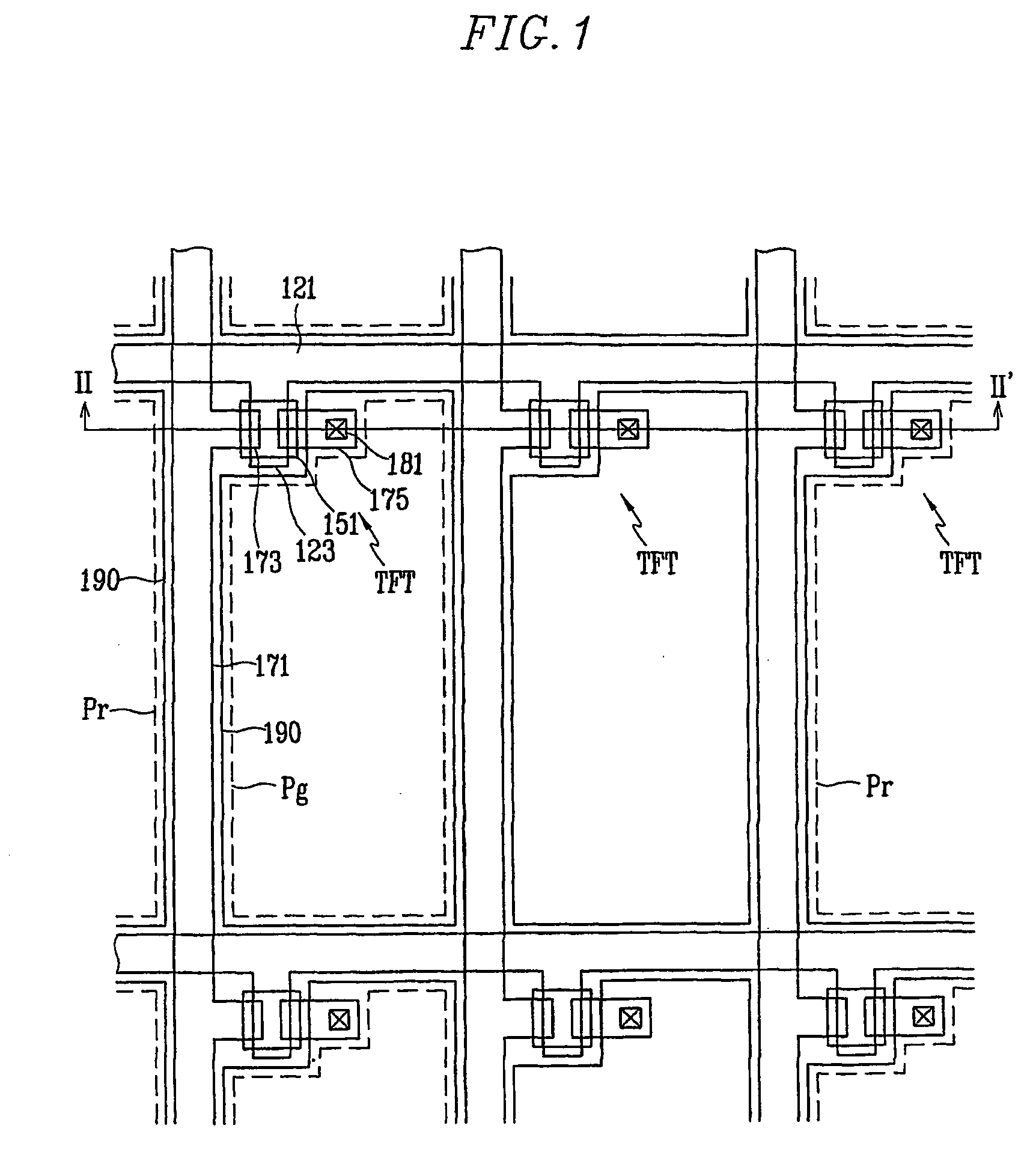
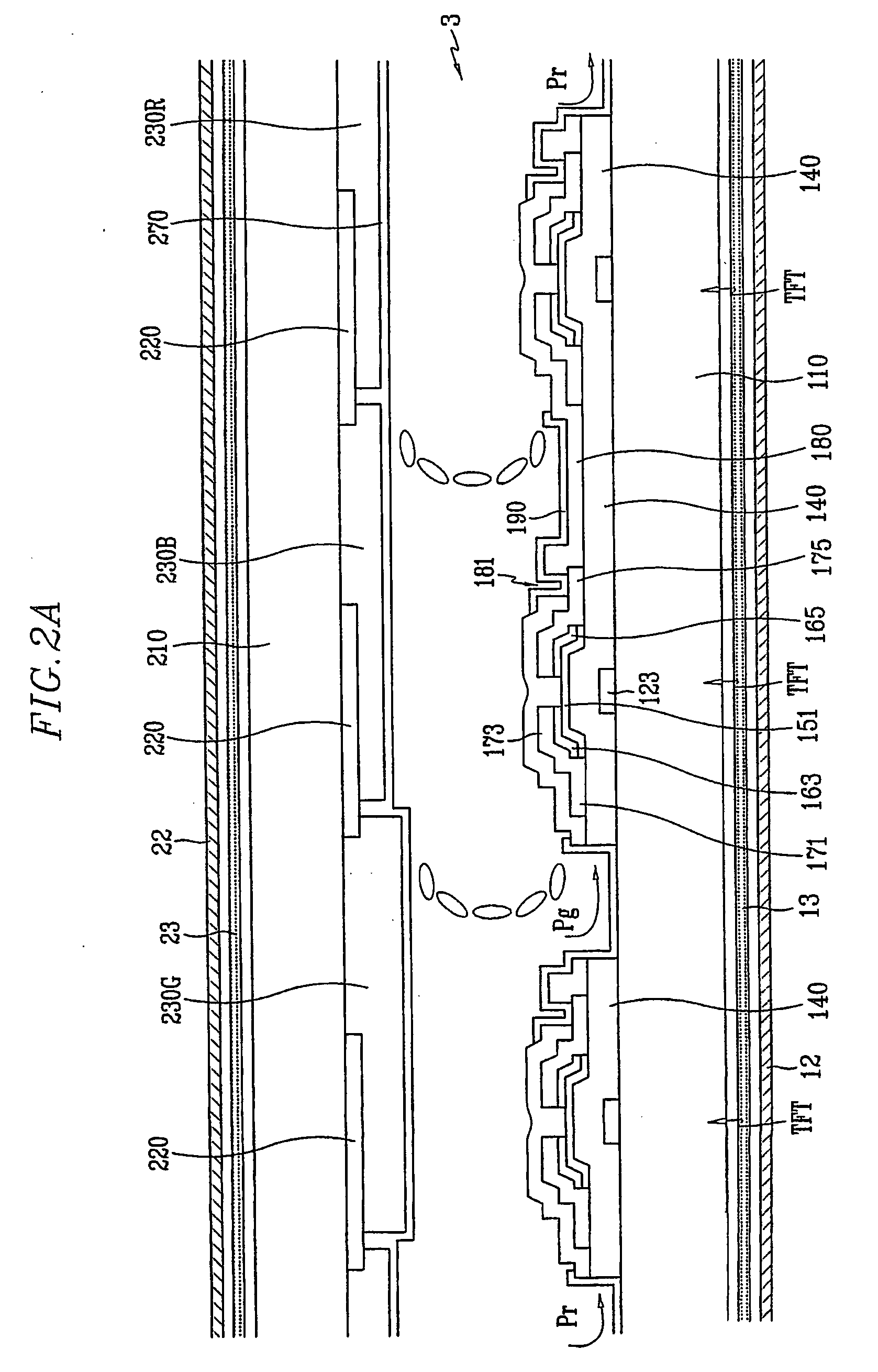
[0029] First, an OCB mode LCD according to the present invention is described with reference to FIGS. 1 and 2A.

[0030] An OCB mode LCD according to this embodiment includes a TFT array panel, a color filter panel, a LC layer 3 interposed between the panels, a pair of compensation films 13 and 23 attached to outer surfaces of the panels, and a pair of polarization films 12 and 22 attached to outer surfaces of the compensation films 13 and 23.

[0031] A TFT array panel is described now.

[0032] A gate wire 121 and 123 preferable made of conductive material such as Al, Al alloy, Cr, Cr alloy, Mo, Mo alloy, Cr nitride, and Mo nitride and having thickness of 1,000-3,500 Å is formed on an insulating substrate 110.

[0033] The gate wire 121 and 123 includes a plurality of gate lines 121 extending in a transverse direction and a plurality of gate electrodes 123 branched from the gate lines 121.

[0034] The gate wire 121 and 123 may have a multi-layered structure including at least two layers, an...

second embodiment

[0056] An OCB mode LCD according to the present invention is described with reference to FIGS. 1 and 2B.

[0057] An OCB mode LCD according to a second embodiment has substantially the same configuration as that according to the first embodiment except that the relation of the cell gap between red, green and blue pixel areas is reversely defined and the wavelength dispersion of the compensation films 13 and 23 is larger than the wavelength dispersion of the LC layer 3. The cell gap according to the second embodiment satisfies the relation:

cell gap in blue pixel area>cell gap in green pixel area>cell gap in red pixel area.

[0058] The second embodiment has an advantage of improving the contrast ratio like the first embodiment.

[0059] The color variation of the cell gap in the first embodiment and the second embodiment is made for compensating the difference between the wavelength dispersion of the LC layer 3 and the wavelength dispersion of the compensation films 13 and 23 and the cell ...

third embodiment

[0079]FIG. 8 is a sectional view of an LCD according to the present invention.

[0080] The third embodiment varies the cell gap by adjusting the thickness of color filters.

[0081] A TFT array panel of an LCD according to the third embodiment will be described.

[0082] A plurality of gate lines (not shown) extending in a transverse direction (not shown), a plurality of storage capacitor lines (not shown) extending parallel to the gate lines, and a plurality of storage electrodes 133a and 133b are formed on an insulating substrate 110 such as transparent glass. A plurality of gate electrodes knot shown) are connected to the gate lines. A gate insulating layer 140 is formed on the gate wire and the storage capacitor wire 133a and 133b and a semiconductor layer (not shown) preferably made of amorphous silicon is formed on the gate insulating layer 140. An ohmic contact layer (not shown) preferably made of amorphous silicon heavily doped with N type impurity such as phosphorous P is formed ...


PUM

PropertyMeasurementUnit
thicknessaaaaaaaaaa
heightaaaaaaaaaa
heightaaaaaaaaaa

Abstract

A liquid crystal display includes a TFT array panel, a color filter panel, a liquid crystal layer in an OCB mode, a pair of compensation films provided on outer surfaces of the TFT array panel and the color filter panel, a pair of polarization films provided on outer surfaces of the compensation films, and so on. When the wavelength dispersion of the liquid crystal layer is larger than the wavelength dispersion of the first and the second compensation films, the cell gap on the red pixel area>the cell gap on the green pixel area>the cell gap on the blue pixel area. On the contrary, when the wavelength dispersion of the liquid crystal layer is smaller than the wavelength dispersion of the first and the second compensation films, the cell gap on the red pixel area<the cell gap on the green pixel area<the cell gap on the blue pixel area.

Description

BACKGROUND OF THE INVENTION [0001] (a) Field of the Invention [0002] The present invention relates to an OCB (Optical Compensated Bend) mode liquid crystal display. [0003] (b) Description of the Related Art [0004] A typical liquid crystal display (LCD) includes an upper panel provided with a common electrode and color filters, etc., a lower panel provided with a plurality of thin film transistors (Ms) and a plurality of pixel electrodes, etc., and a liquid crystal (LC) material interposed between the panels. The pixel electrodes and the common electrode are supplied with different voltages to generate electric field changing the orientations of LC molecules, thereby controlling light transmittance to display images. [0005] An OCB mode LCD among the LCDs has advantages in wide viewing angle and fast response and, recently, it has been actively studied for application. However, an OCB mode LCD has a problem of low contrast ratio. It is because the OCB mode LCD gives relatively high lu...

Claims


Application Information

Patent Timeline
Patent Type & Authority Applications(United States)
IPC IPC(8): G09G3/36G02F1/1335G02F1/13363G02F1/139
CPCG02F1/133514G02F1/1395G09G2320/0242G09G3/2003G09G3/3607G02F2413/09G02F1/133631G02F1/1335
Inventor SONG, JANG-KUNLEE, CHANG-HUN
Owner SAMSUNG DISPLAY CO LTD
Why Eureka
Try Eureka