Liquid crystal driving device, liquid crystal display device, and liquid crystal driving method

a driving device and liquid crystal technology, applied in the direction of instruments, static indicating devices, etc., can solve the problems of not only but also the inability to control the application voltage vsub>lc/sub>, so as to suppress the flickering of the display image and suppress the flickering of the image

Inactive Publication Date: 2006-07-13
RENESAS ELECTRONICS CORP
View PDF3 Cites 41 Cited by
  • Summary
  • Abstract
  • Description
  • Claims
  • Application Information

AI Technical Summary

Benefits of technology

[0019] The above structure or driving method of the present invention makes it possible to change a common electrode voltage value in consideration of a timing of displaying an image on the liquid crystal display panel. Accordingly, a preset value of the common electrode voltage can be changed during such a period that no image is displayed on the liquid crystal display panel. Consequently, it is possible to suppress flickering in a display image due to the abrupt luminance change.
[0020] According to the present invention, it is possible to provide a liquid crystal driving device, a liquid crystal display device, and a liquid crystal driving method, which can suppress the flickering in an image displayed on a liquid crystal display panel by controlling a timing of changing a level of voltage applied to the common electrode.

Problems solved by technology

If a DC voltage is continuously applied to the liquid crystal, a liquid crystal element could burn out and deteriorate.
Such a difference between the negative polarity and the positive polarity of the liquid crystal application voltage VLC causes not only flickering of a display image but burning due to the application of the DC voltage to the liquid crystal.
However, the known liquid crystal display device has a problem that a timing of adjusting the value of the common voltage Vcom for removing the DC components of the liquid crystal application voltage VLC cannot be controlled.
Hence, it is difficult for the structure disclosed in Japanese Unexamined Patent Application Publication No. 2000-267618 to adjust the common voltage Vcom under control exclusively during a blanking period in which neither data lines nor gate lines in a display area of the liquid crystal display panel are driven.
If the common voltage Vcom is changed during a period (scanning period) in which an image is being displayed on the liquid crystal display panel, without controlling the timing of adjusting the common voltage Vcom, flickering occurs in a display image due to an abrupt luminance change, leading to deterioration of an image quality.

Method used


Image

  • Liquid crystal driving device, liquid crystal display device, and liquid crystal driving method
  • Liquid crystal driving device, liquid crystal display device, and liquid crystal driving method
  • Liquid crystal driving device, liquid crystal display device, and liquid crystal driving method

Examples


first embodiment

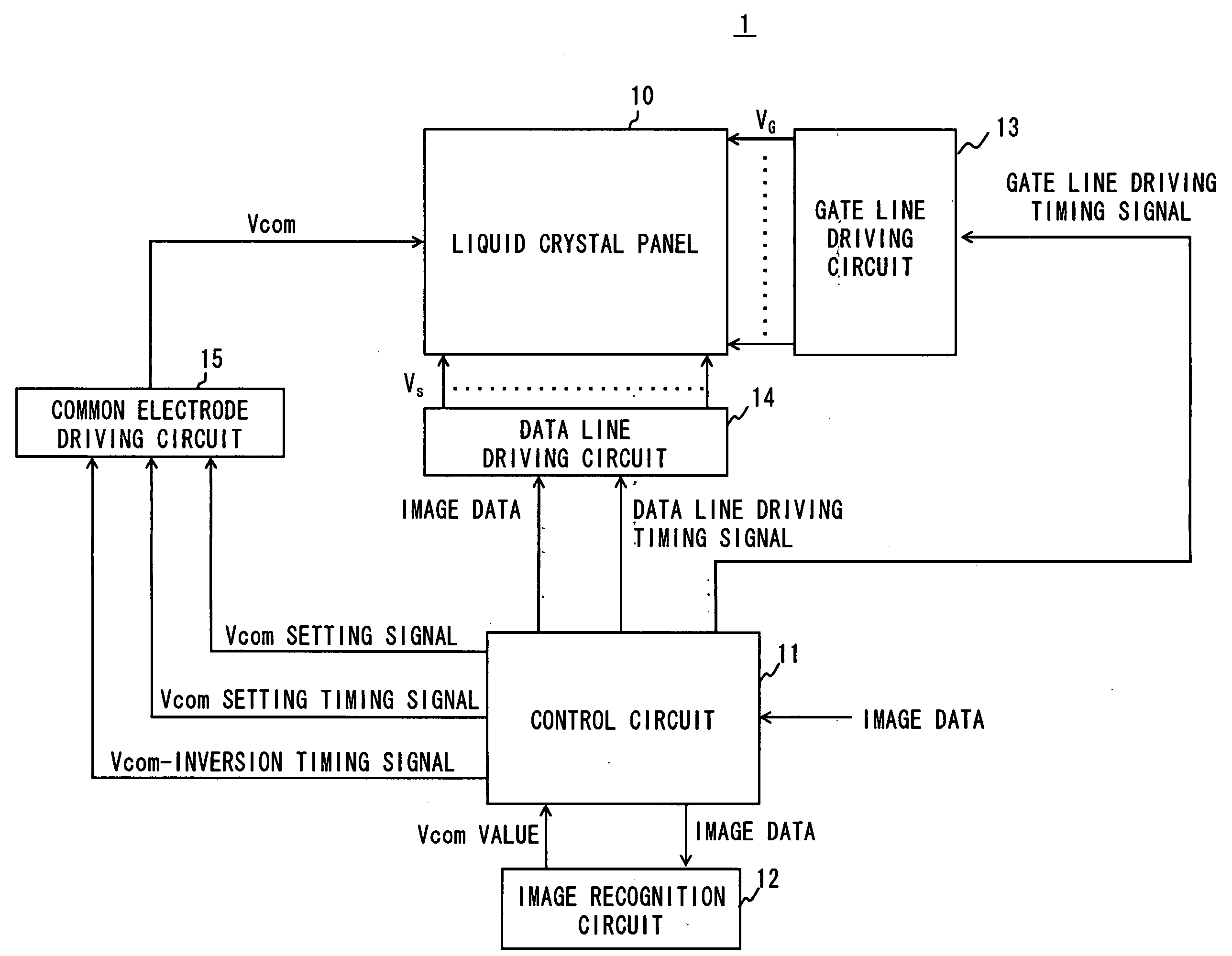
[0038] Referring to FIG. 1, the structure of a liquid crystal display device 1 according to a first embodiment of the present invention is described. A liquid crystal display panel 10 is an active matrix type liquid crystal display panel using a TFT as a switching element, and has the same structure as the liquid crystal display panel of the related art illustrated in FIG. 13. In short, in the liquid crystal display panel 10, plural gate lines 111 and plural data lines 112 are arranged in matrix. At intersections between the gate lines 111 and the data lines 112, liquid crystal pixels are provided, which includes a TFT 110, a pixel electrode 113, a common electrode 114, a liquid crystal capacitor CLC, and an auxiliary capacitor Cs. The liquid crystal display panel 10 is driven with a gate voltage VG, source voltage VS, and common voltage Vcom applied by a gate line driving circuit 13, a data line driving circuit 14, and a common electrode driving circuit 15, respectively.

[0039] A c...

example 1

FIG. 6

[0055] First of all, the gray scales of the image data are prioritized in advance. For example, the gray scale where flickering noticeably occurs due to the difference between the positive polarity and the negative polarity of the liquid crystal application voltage VLC is given a high priority. The gray scale where flickering is less noticeable is given a low priority. At the time of determining the Vcom set value, the gray scale that is given the highest priority of all gray scales in the image data is selected (step S601), and the Vcom set value corresponding to the gray scale of the highest priority is selected with reference to the relation between the gray scale initially set in step S401 and the Vcom set value (step S602). Note that all the gray scales may be prioritized, but only the gray scales that are particularly susceptible to flickering may be prioritized without prioritizing the remaining gray scales, and a uniform value is set as the Vcom set value for the remai...

example 2

FIG. 7

[0056] First, the gray scale that is most frequently used (appears at a high frequency) of all gray scales in the image data is selected (step S701). Then, the Vcom set value corresponding to the gray scale of the highest frequency is selected with reference to the relation between the gray scale initially set in step S401 and the Vcom set value (step S702).

[0057] Hence, the common voltage Vcom can be corrected in accordance with the gray scale of the highest frequency of appearance, in short, the most noticeable gray scale, so an image that is reduced flickers can be displayed.


PUM


Abstract

A liquid crystal display device according to an embodiment of the present invention includes an active matrix type liquid crystal display panel, in which a set value of a common voltage applied to a common electrode of the liquid crystal display panel is determined based on input image data, and a timing of changing the common voltage to the preset value in accordance with a timing of driving at least one of a scan line and a signal line of the liquid crystal display panel.

Description

BACKGROUND OF THE INVENTION [0001] 1. Field of the Invention [0002] The present invention relates to a liquid crystal driving device and method, and a liquid crystal display device for driving an active matrix type liquid crystal display panel. [0003] 2. Description of Related Art [0004] Active matrix type liquid crystal display panels such as a TFT liquid crystal display panel have switching elements such as a TFT, liquid crystal capacitors CLC, and an auxiliary capacitor CS at intersections between gate lines (scan lines) and data lines (signal lines) arranged in matrix. The following description focuses on the TFT liquid crystal display panel by way of example. FIG. 13 shows an equivalent circuit of the TFT liquid crystal display panel. [0005] A TFT 110 has a gate electrode G connected to a gate line 111, a source electrode S connected to a data line 112, and a drain electrode D connected to a pixel electrode of the liquid crystal capacitors CLC and the auxiliary capacitor CS. Th...

Claims


Application Information

Patent Timeline
Patent Type & Authority Applications(United States)
IPC IPC(8): G09G3/36
CPCG09G3/3655G09G2320/0247G09G2360/16
Inventor FURIHATA, HIROBUMINOSE, TAKASHI
Owner RENESAS ELECTRONICS CORP
Why Eureka
Try Eureka