

Image Display Device and Method of Testing the Same
a display device and image technology, applied in the direction of static indicating devices, non-linear optics, instruments, etc., can solve the problem of expensive testing apparatus, and achieve the effect of easy testing in a short tim
- Summary
- Abstract
- Description
- Claims
- Application Information
AI Technical Summary
Benefits of technology
Problems solved by technology
Method used
Image

Examples
embodiment mode 1
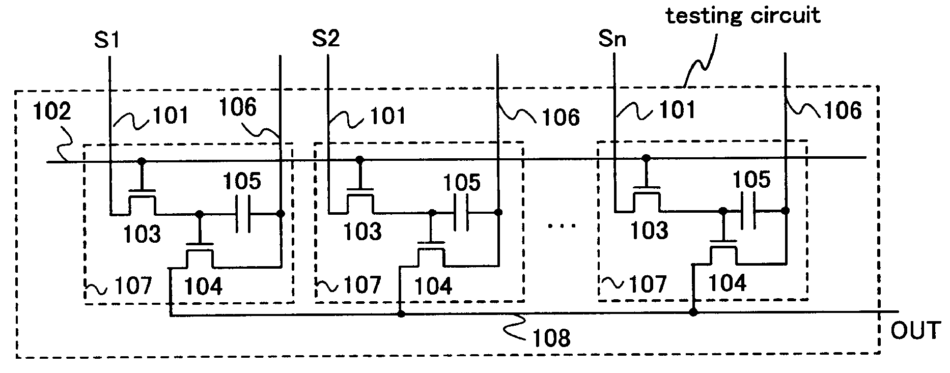
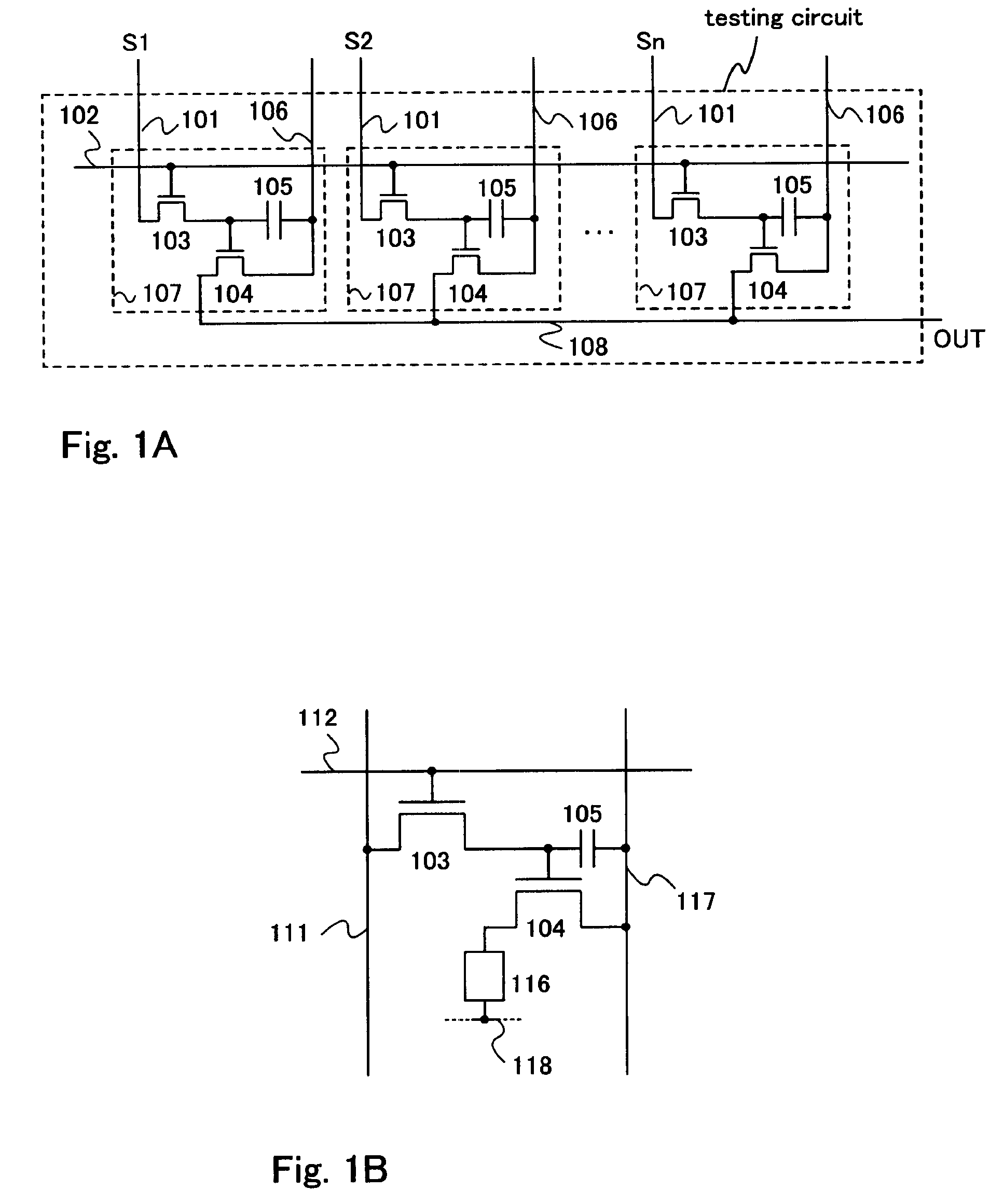
[0034]FIG. 1A shows a testing circuit according to the embodiment mode 1 of the invention. The testing circuit comprises a data signal line 101, a scanning line 102, a switching TFT 103, a driver TFT 104, a capacitor 105, a current supply line 106, a testing cell 107, and a testing line 108. The circuit of FIG. 1A is used for testing data signal lines. The testing circuit comprises a pixel circuit as shown in FIG. 1B and the testing cell 107 corresponds to the pixel circuit. The pixel circuit of FIG. 1B comprises a data signal line 111, a scanning line 112, a switching TFT 103, a driver TFT 104, a capacitor 105, an EL element 116, a current supply line 117, and a power source line 118.
[0035] In the pixel circuit, the driver TFT 104 supplies a current to the EL element 116 to emit light. The EL element 116 emits light in accordance with a potential of a video signal which is inputted to a gate of the driver TFT 104 from the source signal line 111 through the switching TFT 103.
[0036...
embodiment mode 2
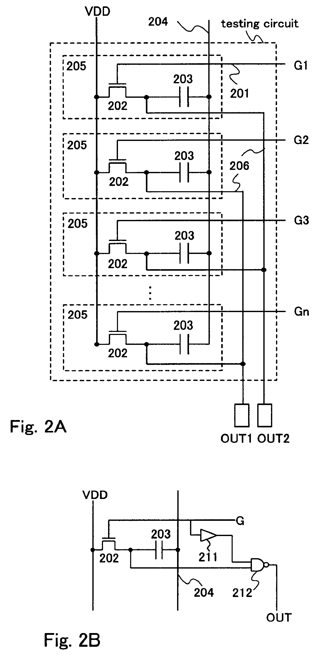
[0039]FIGS. 2A and 2B each shows a testing circuit according to the embodiment mode 2 of the invention. This circuit is used for the test of scanning lines. The testing circuit is prepared based on the pixel circuit of FIG. 1B as in embodiment mode 1, and a testing cell 205 in FIG. 2A corresponds to the pixel circuit.
[0040] The testing circuit in FIG. 2A comprises a scanning line 201, a switching TFT 202, a capacitor 203, a current supply line 204, a testing cell 205, and a testing line 206.
[0041] The configuration of the testing cell 205 is explained by comparison with a pixel circuit. An EL element and a driver TFT are removed from a pixel circuit. The power source line 118 connected to the EL element is detached from the drier TFT 104 and connected to the testing line 206. Also, the data signal line 111 shared by pixel circuits is detached from the source driver circuit and connected to the power voltage VDD, thereby the testing cell 205 is obtained. The switching TFT operates ...
embodiment 1
[0047]FIG. 5A shows embodiment 1 of the invention. A display device shown here comprises a substrate 501, a source driver circuit 502, a gate driver circuit 503, a pixel 504, a data signal line 505, and a scanning line 506. Among the pixels arranged in matrix, the last row of pixels opposed to the source driver circuit 502 is selected. In the case where dummy pixels are arranged in the periphery of a display region, they may be selected. The selected pixels are changed as follows. The EL element is removed from the pixel and the TFT in the pixel is detached from the power source line which is connected to the EL element, and connected to a testing terminal instead. One testing terminal is employed in the embodiment of FIG. 5A by connecting all the pixels in the row in common, although testing terminals may be plural if needed for the testing reason. Further, the scanning line 506 shared by pixels is detached from the gate driver circuit 503 so that an independent switch signal line ...
PUM
 Abstract
Description
Claims
Application Information