Method for manufacturing perovskite type oxide layer, method for manufacturing ferroelectric memory and method for manufacturing surface acoustic wave element
a technology of ferroelectric memory and perovskite type, which is applied in the direction of fixed capacitors, thin/thick film capacitors, devices, etc., can solve the problems of excessive defects may be generated in perovskite type crystal structure, and insufficient characteristics and reliability of devices, etc., to achieve excellent interface
- Summary
- Abstract
- Description
- Claims
- Application Information
AI Technical Summary
Benefits of technology
Problems solved by technology
Method used
Image

Examples
first embodiment
1. First Embodiment
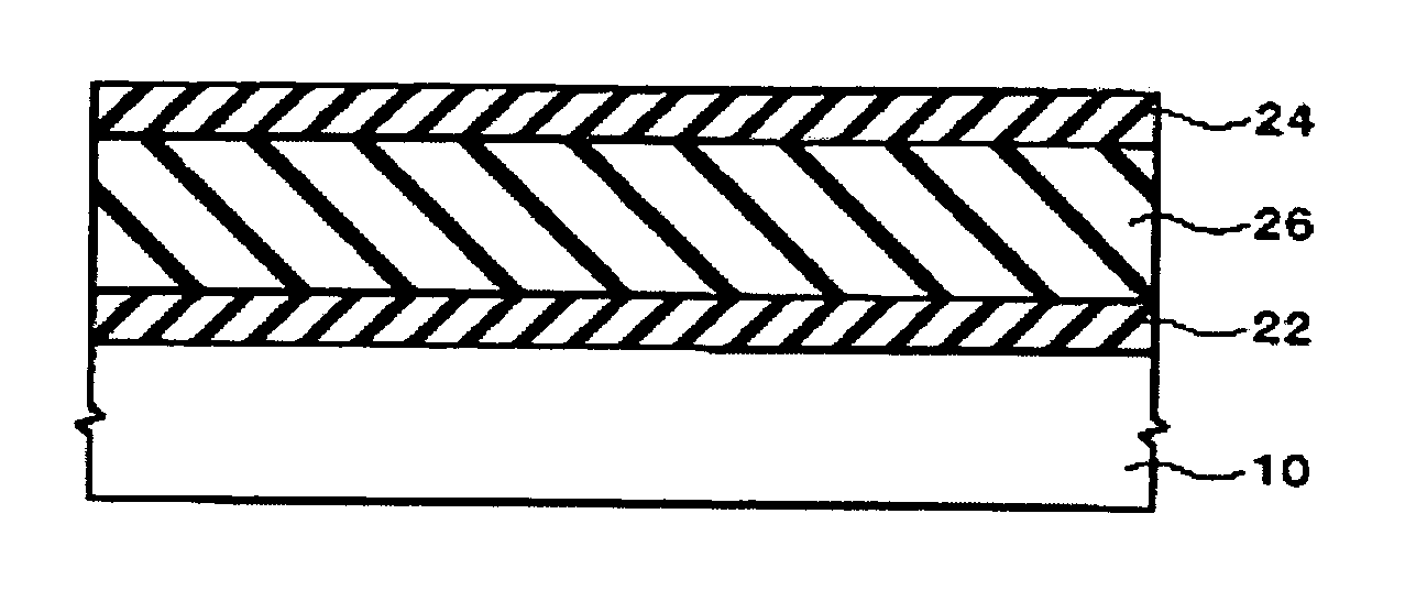
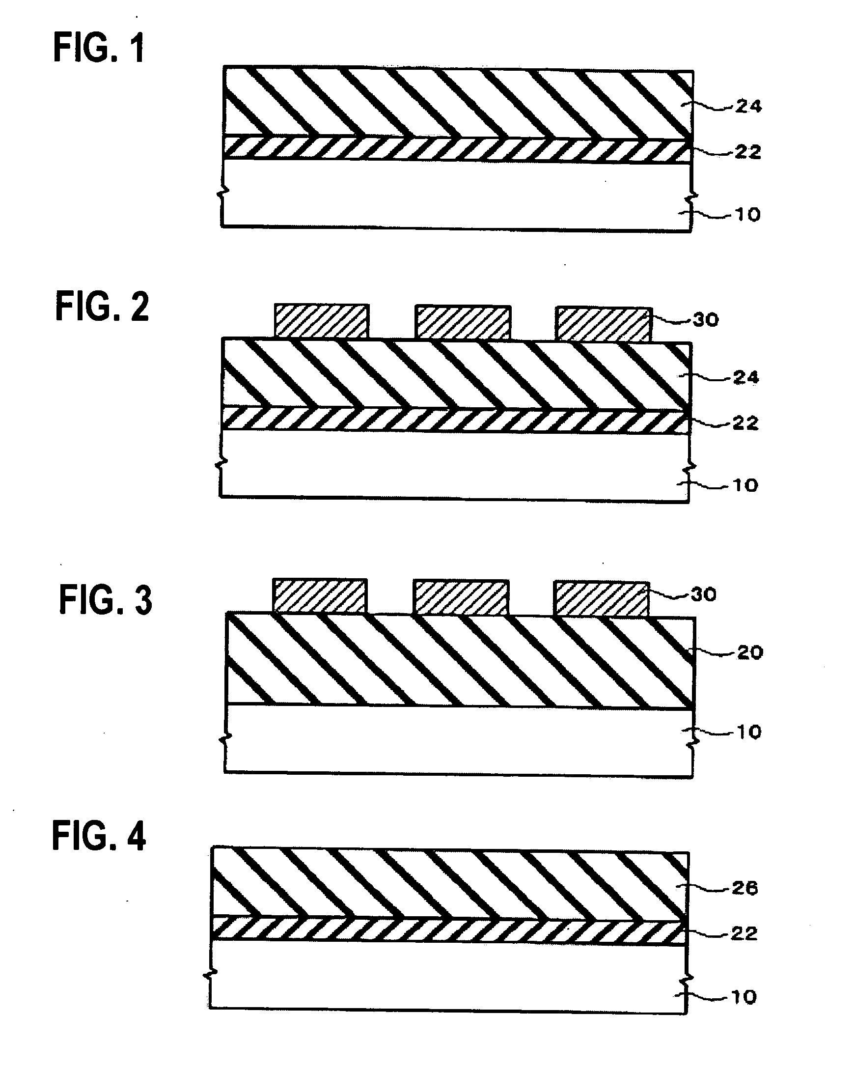
[0030]FIGS. 1 through 3 are cross-sectional views schematically showing steps of a manufacturing method in accordance with an embodiment of the invention.
[0031] (1) First, as shown in FIG. 1, a first oxide layer 22 is formed on a substrate 10. The first oxide layer 22 is formed with a crystal orientation of a perovskite type oxide layer that is to be finally obtained.
[0032] For example, the first oxide layer may be formed by epitaxial growth with respect to the substrate 10. In this case, the first oxide layer 22 grows with the same orientation as that of the substrate 10. As the substrate 10, a single crystal substrate, or a base material (not shown) with a so-called buffer layer having a crystal controllability formed thereon.
[0033] Any one of substrates in a variety of types can be used as the substrate 10 depending on the type and usage of the perovskite type oxide layer. For example, when the perovskite type oxide layer is used as a capacitor of a device s...
second embodiment
2. Second Embodiment
[0056]FIG. 4 is a cross-sectional view schematically showing a step of a manufacturing method in accordance with a second embodiment of the invention. It is noted that members shown in FIG. 4 that are substantially the same as those of the first embodiment are appended with the same reference numbers, and their detailed description is omitted. The present embodiment differs from the first embodiment in that perovskite type oxide is used to compose a second oxide layer.
[0057] (1) First, as shown in FIG. 4, a first oxide layer 22 is formed on a substrate 10. The first oxide layer 22 is formed to have a crystal orientation of a perovskite type oxide (also hereafter referred to as “first perovskite type oxide”) layer that is desired to be finally obtained. The substrate 10 is similar to the substrate in the first embodiment.
[0058] (2) Next, as shown in FIG. 4, a second oxide layer 26 composed of second perovskite type oxide is formed on the first oxide layer 22.
[0...
third embodiment
3. Third Embodiment
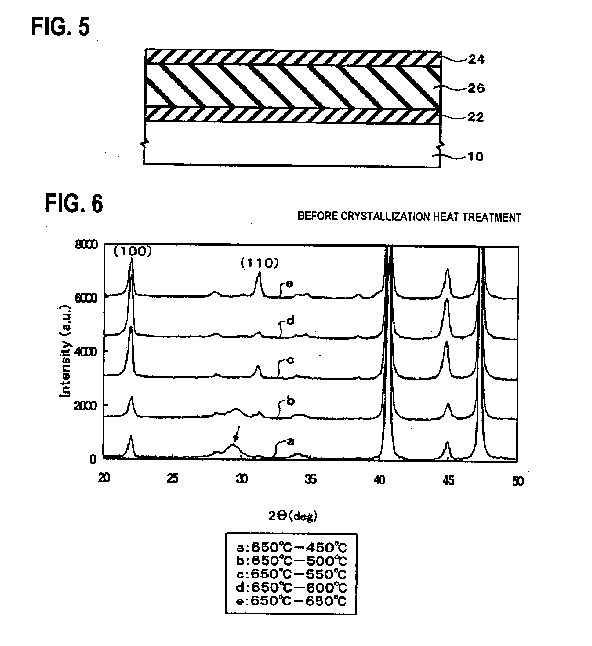
[0076]FIG. 5 is a cross-sectional view schematically showing a step of a manufacturing method in accordance with a third embodiment of the invention. It is noted that members shown in FIG. 5 that are substantially the same as those of the first embodiment shown in FIG. 1 and the second embodiment shown in FIG. 4 are appended with the same reference numbers, and their detailed description is omitted.
[0077] The present embodiment differs from the first embodiment or the second embodiment in that both of a perovskite type oxide layer and a pyrochlore layer are used as a second oxide layer.
[0078] (1) First, as shown in FIG. 5, a first oxide layer 22 is formed on a substrate 10. The first oxide layer 22 is formed to have a crystal orientation of a perovskite type oxide (also hereafter referred to as “first perovskite type oxide”) layer that is to be finally obtained. The substrate 10 is similar to the substrate in the first embodiment.
[0079] (2) Next, as shown in FI...
PUM
| Property | Measurement | Unit |
|---|---|---|
| temperature | aaaaa | aaaaa |
| temperature | aaaaa | aaaaa |
| temperature | aaaaa | aaaaa |
Abstract
Description
Claims
Application Information
 - R&D Engineer
- R&D Manager
- IP Professional
- Industry Leading Data Capabilities
- Powerful AI technology
- Patent DNA Extraction
Browse by: Latest US Patents, China's latest patents, Technical Efficacy Thesaurus, Application Domain, Technology Topic.
© 2024 PatSnap. All rights reserved.Legal|Privacy policy|Modern Slavery Act Transparency Statement|Sitemap