Apparatus and method for data processing for IC tags and image forming device with the apparatus

a technology of image forming device and apparatus, which is applied in the field of apparatus and method for data processing of ic tags and image forming devices, can solve the problems of uncompleted reading and/or writing of information, inability to identify, and communication errors,

Active Publication Date: 2006-10-26
KONICA MINOLTA BUSINESS TECH INC
View PDF9 Cites 20 Cited by
  • Summary
  • Abstract
  • Description
  • Claims
  • Application Information

AI Technical Summary

Benefits of technology

[0012] It is a primary object of this invention to provide an apparatus and method for data processing for IC tags, wherein the apparatus and method set up a state that enables reliable radio communication with a plurality of IC tags mounted on a conveying medium and read and / or write electronic information from / to the IC tags, and to provide an image forming device capable of recording an image onto the conveying medium on which the IC tags are mounted.

Problems solved by technology

Furthermore, when the conveying medium on which IC tags are mounted is moved at a constant speed, if the amount of data for electronic information to be read from and / or written to an IC tag is great, reading and / or writing of the information may be uncompleted during the passage of the IC tag through the antenna coverage of the reader / writer.
When a plurality of IC tags exist in the antenna coverage of the reader / writer, an IC tag for which reading and / or writing of electronic information should be performed cannot be identified and a communication error may take place.
The use of a smaller antenna for countermeasures against such error may result in incompletion of reading and / or writing of electronic data during the passage through the antenna coverage.
The above prior art readers / writers that read and / or write electronic information from / to IC tags each bring about disadvantages below: need for the mechanism to move the antenna orthogonally to the direction in which IC tags are conveyed (Japanese Laid Open Patent Publication No. 2003-300356); provision of multiple antennas for countermeasures against communication errors which may occur when a plurality of IC tags exist in the antenna coverage of the reader / writer; and need for communication error preventing measures such as providing more spacing between IC tags on the conveying medium in the conveyance direction.

Method used


Image

  • Apparatus and method for data processing for IC tags and image forming device with the apparatus
  • Apparatus and method for data processing for IC tags and image forming device with the apparatus
  • Apparatus and method for data processing for IC tags and image forming device with the apparatus

Examples


first embodiment

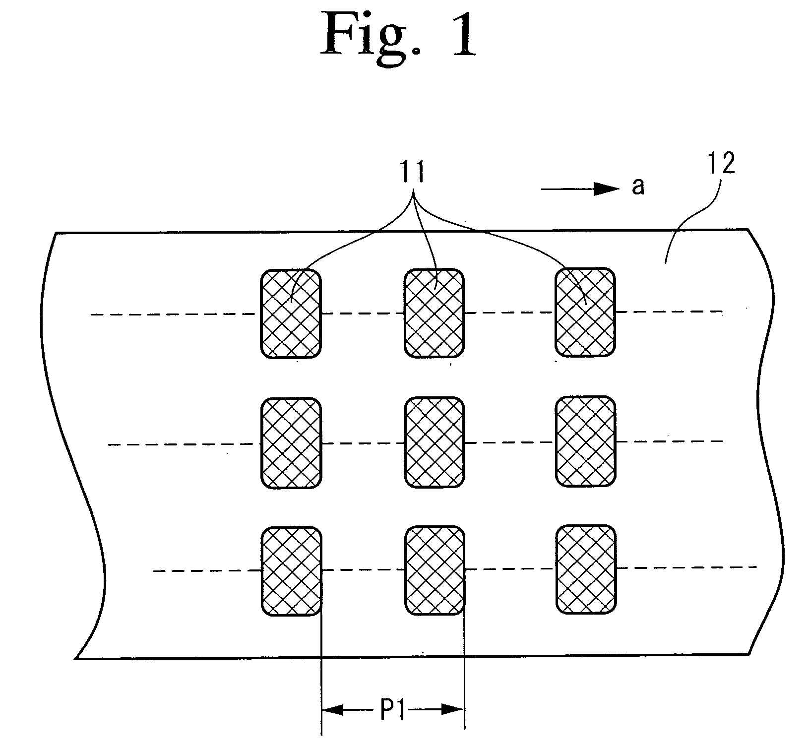
[0031]FIG. 1 is a front view of a conveying medium on which IC tags are mounted. Wireless communication devices (hereinafter referred to as IC tags) 11, which will be described later, are mounted on the medium, arranged at fixed pitch p1 in multiple rows (three rows in FIG. 1) in parallel with the direction of arrow a in which the conveying medium 12 moves (the direction of conveyance of the IC tags) and in multiple columns along the direction of arrow a. The conveying medium 12 is, for example, continuous-form paper or other similar media for use in a label printer or the like, on which visible information such as desired text is printed. After electronic information is read from and / or written to the IC tags 11 by a data processing apparatus which will be described later, the medium is cut into labels with predetermined dimensions and each label having an IC tag will be stuck to a commercial product or the like. Although, by way of example, labels are produced in this embodiment, ...

second embodiment

[0072] A data processing apparatus of a second embodiment of the invention has the same reader / writer and antenna as in the first embodiment, but the antenna is not skewed. Instead, by modifying the arrangement of the IC tags on the conveying medium, each IC tag can be identified. Components corresponding to those described in the first embodiment are assigned the same reference numbers and their explanation is not repeated. The following description of the second embodiment focuses on difference from the first embodiment.

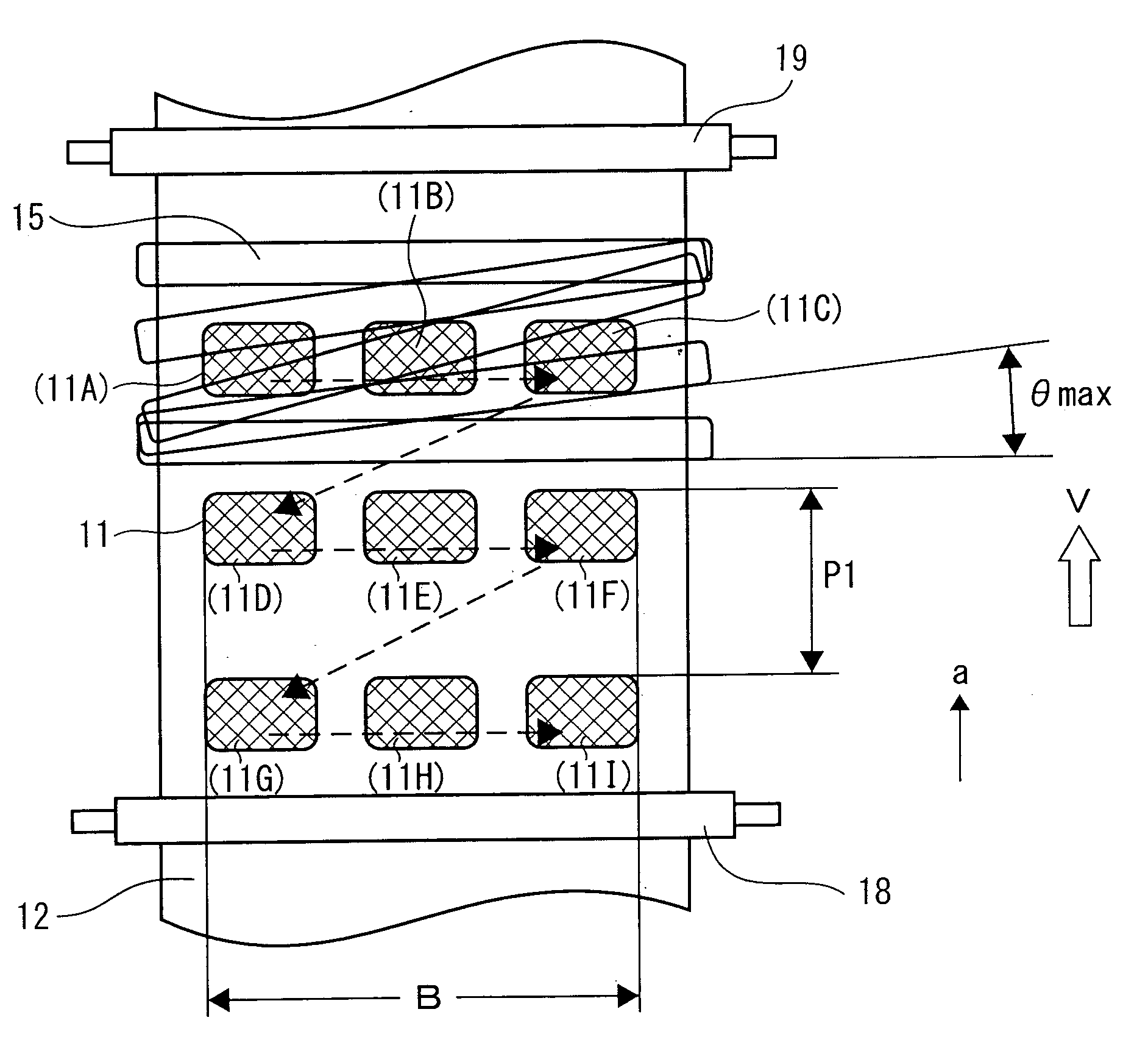
[0073] In the data processing apparatus 10 of the first embodiment, a plurality of IC tags 11 are arranged in multiple rows and columns along the direction of arrow a in which the conveying medium and the IC tags move, as shown in FIG. 6, and the apparatus is configured so that each IC tag 11 will be identified by skewing the antenna 15 of the reader / wrier 14 at the angle θ.

[0074]FIG. 9 is a diagram to explain how IC tags 11 are arranged on the conveying medium 1...

third embodiment

[0077] This section describes a data processing apparatus of a third embodiment of the invention. The above-described data processing apparatus of the first embodiment fixes the skew angle of the reader / writer antenna to a predetermined angle θ determined by calculation and reads and / or writes electronic information from / to IC tags being conveyed. On the other hand, in the third embodiment, the apparatus reads and / or writes electronic information from / to IC tags, while changing the skew angle of the reader / writer antenna in conjunction with the conveyance of the IC tags. The data processing apparatus of the third embodiment is capable of identifying each IC tag positively and reliable reading and / or writing of electronic information, even if a plurality of IC tags are arranged closely with each other on the conveying medium.

[0078]FIG. 10 is a diagram to explain identifying IC tags and sequence in which reading / writing of electronic information from / to the tags will be performed, ac...


PUM


Abstract

The invention relates to an apparatus and method for data processing for IC tags and an image forming device capable of recording an image onto a conveying medium on which IC tags are mounted. The apparatus and method set up a state that enables reliable radio communication between a reader/writer and an IC tag and read and/or write electronic information from/to IC tags. The reader/writer's antenna to face IC tags mounted on the conveying medium, arranged in multiple rows and columns in the conveyance direction, is skewed so that the IC tags pass sequentially under the antenna and each IC tag can be identified. The reader/writer reads and/or writes electronic information associated with the thus identified IC tag.

Description

[0001] This application is based on application No. 2005-126360 filed in Japan, the contents of which are hereby incorporated by reference. BACKGROUND OF THE INVENTION [0002] 1. Field of the Invention [0003] This invention relates to an apparatus and method for data processing for IC tags and an image forming device such as a label printer. In particular, the invention relates to an apparatus and method for data processing for IC tags by which electronic information is read from and / or written to IC tags moving in a given direction, the IC tags being transported by a conveying medium on which they are mounted, and an image forming device with the data processing apparatus for IC tags. [0004] 2. Prior Art [0005] A wireless communication device comprising a storage device, a transceiver, and an antenna is a semiconductor device from / to which contactless reading and / or writing of electronic information can be performed, which is generally called a Radio Frequency Identification (RFID) ...

Claims


Application Information

Patent Timeline
Patent Type & Authority Applications(United States)
IPC IPC(8): G06K7/00G06K7/08
CPCG06K7/10336G06K7/10435G06K2017/0038G06K17/0025G06K7/10455
Inventor SHIIGI, MASAHIROOHARA, KOUJINOMURA, TAKESHITAMADA, TAKESHITOKUAN, HIROSHI
Owner KONICA MINOLTA BUSINESS TECH INC
Why Eureka
Try Eureka