

Received data compensating device
- Summary
- Abstract
- Description
- Claims
- Application Information
AI Technical Summary
Benefits of technology
Problems solved by technology
Method used
Image

Examples
first embodiment
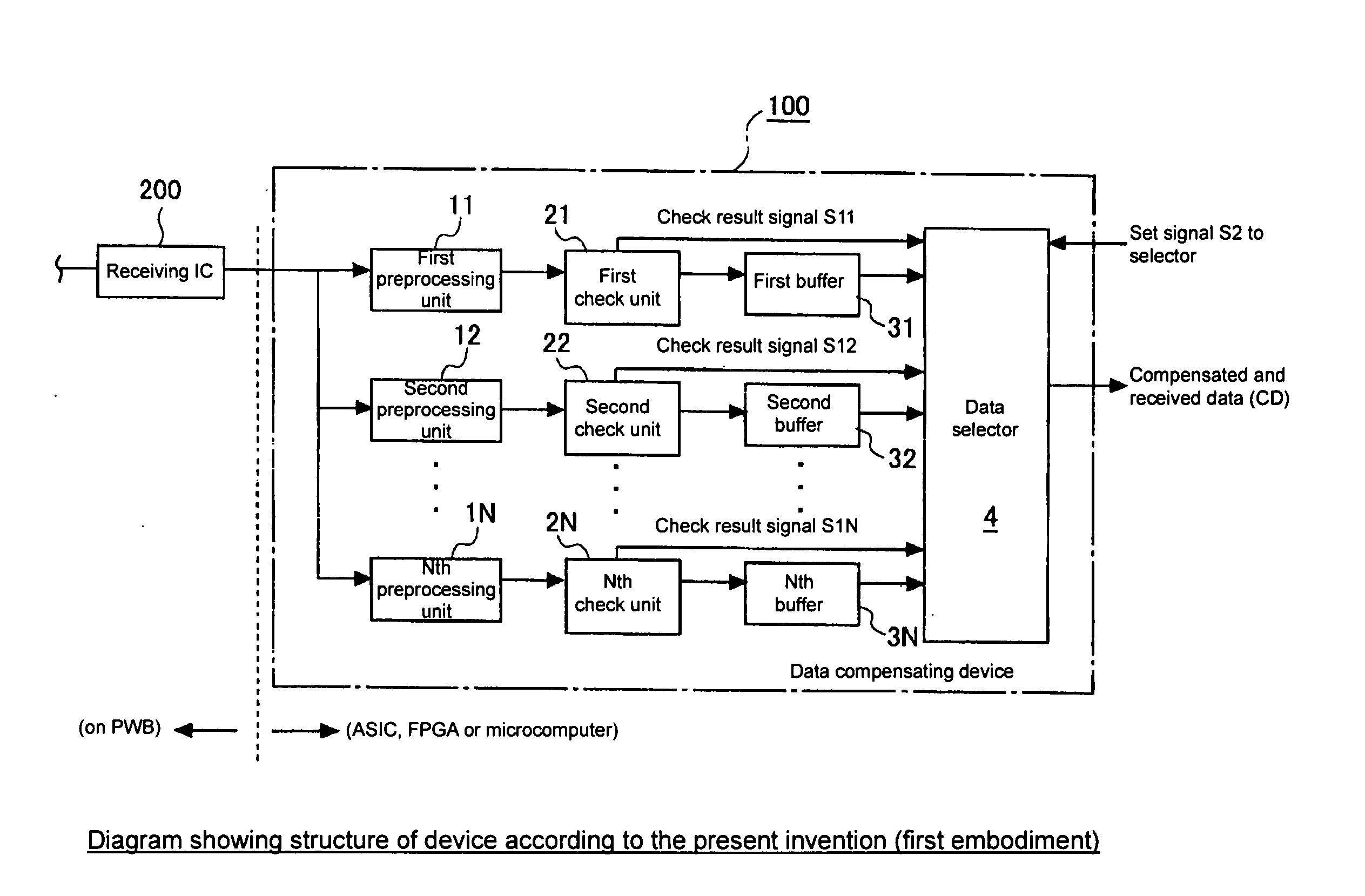
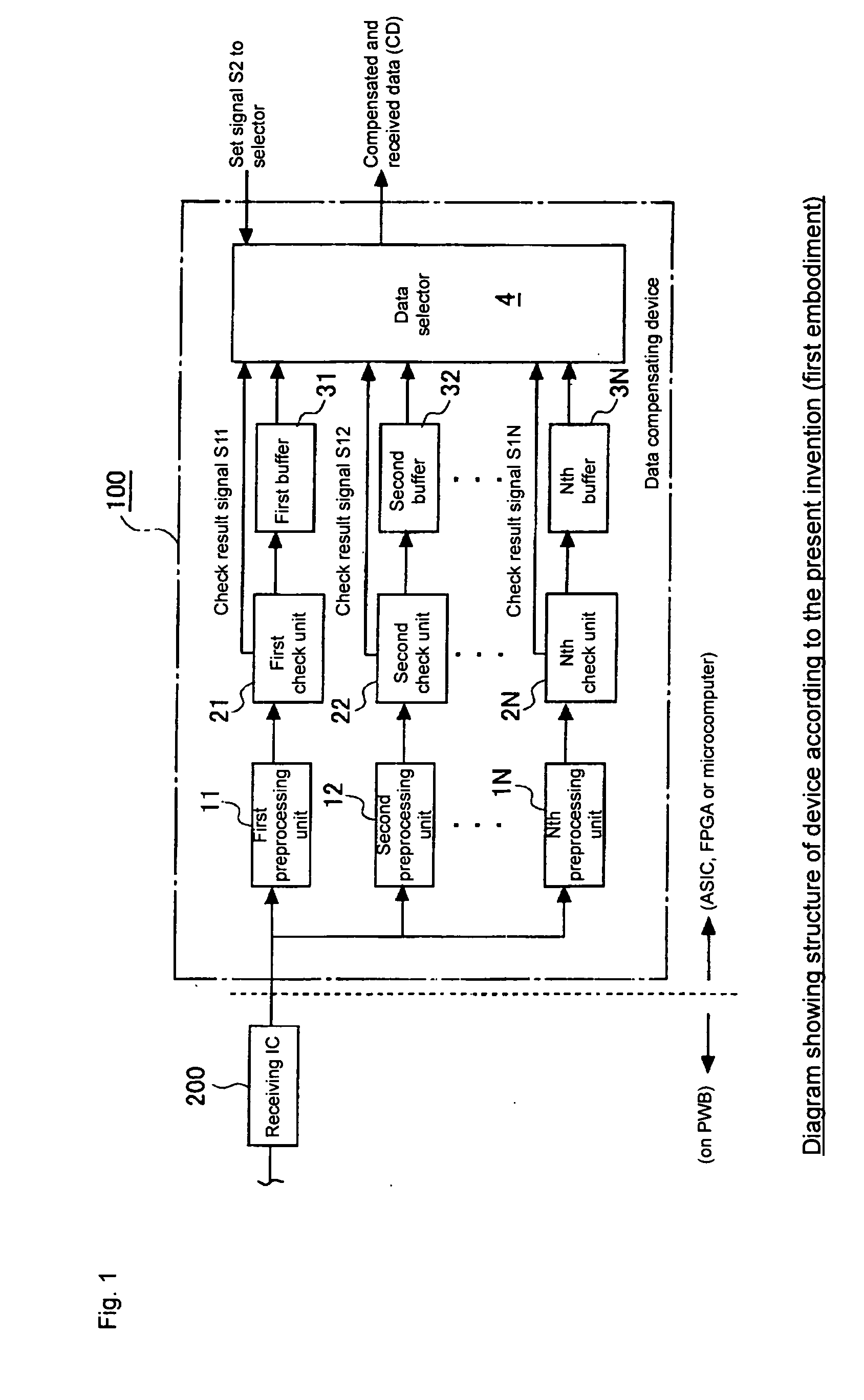
[0031] An embodiment of a received data compensating device according to the present invention will be described below in detail with reference to the accompanying drawings. FIG. 1 is a diagram showing a structure of the device according to the present invention (a first embodiment).
[0032] As shown in FIG. 1, a received data compensating device 100 according to the present invention is provided in a rear stage of a receiving IC 200 constituting a physical layer. It is possible to utilize the RS485 specification for the receiving IC 200, for example. More specifically, AD485 of analog devices and the like are suitable. In this example, the receiving IC 200 is mounted on a printed wiring board.
[0033] On the other hand, the received data compensating device 100 according to the present invention has the following structure. More specifically, the received data compensating device 100 according to the present invention comprises a plurality of preprocessing units 11, 12, . . . 1N provi...
second embodiment
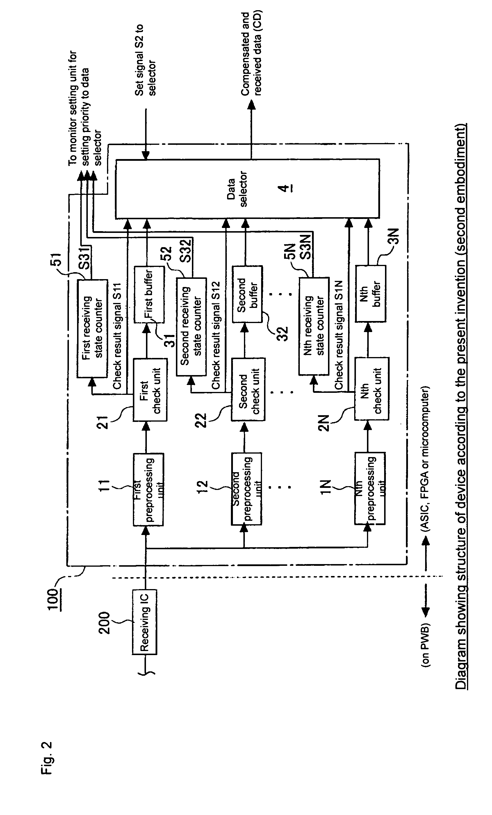
[0044]FIG. 2 shows a diagram showing a structure of the device according to the present invention (a second embodiment). FIGS. 2 and 1 are different from each other in that receiving state counters 51, 52, . . . 5N for counting receiving state signals (abnormal or normal) generated from the first check unit 21, the second check unit 22, . . . the Nth check unit 2N respectively are provided, count signals S31, S32, . . . S3N obtained from their counters are sent to a monitor setting unit for setting a priority to the data selector, and the priority in the data selector is reset based on the their count results.
[0045] The received data compensating device 100 according to the present invention can be incorporated into various receiving apparatuses constituting the PLC system.
[0046]FIG. 3 shows a diagram showing a structure of a master unit (or a slave unit) in which the device according to the present invention is incorporated. As shown FIG. 3, in this example, the received data comp...
PUM
 Abstract
Description
Claims
Application Information