Method for fabricating thin film transistor (TFT) display

a thin film transistor and display technology, applied in the field of thin film transistor display methods, can solve problems such as lowering yield, and achieve the effect of improving yield and varied tft display modes

Inactive Publication Date: 2006-12-07
IND TECH RES INST
View PDF0 Cites 5 Cited by
  • Summary
  • Abstract
  • Description
  • Claims
  • Application Information

AI Technical Summary

Benefits of technology

[0007] In view of the above problems, an object of the invention is to provide a method for fabricating a TFT display, wherein using the property of polymeric material, the display substrate and TFT substrate can be combined together by laminating after separate process, thereby achieving the improved yield and varied TFT display modes, and substantially solving the problems in the prior art.
[0009] Wherein, since the protective layer of the TFT substrate is a polymeric material, which is selected from thermoset or photopolymerizable materials, the polymeric material is cured and polymerized through heating and illuminating, to combine with the liquid crystal substrate. In addition, the step of removing the sacrificial layer has made the bottom layer of the liquid crystal substrate into a polymer layer, and the bottom layer of the TFT substrate of the present invention may also be made of polymer, therefore the flexibility of the TFT display can be improved, and various TFT display modes can be increased.

Problems solved by technology

However, its disadvantage resides in that the display section cannot be fabricated until the fabrication of the OTFT is finished, and the OTFT section might be damaged while fabricating the display section, thereby resulting in a lowered yield.

Method used


Image

  • Method for fabricating thin film transistor (TFT) display
  • Method for fabricating thin film transistor (TFT) display
  • Method for fabricating thin film transistor (TFT) display

Examples


Embodiment Construction

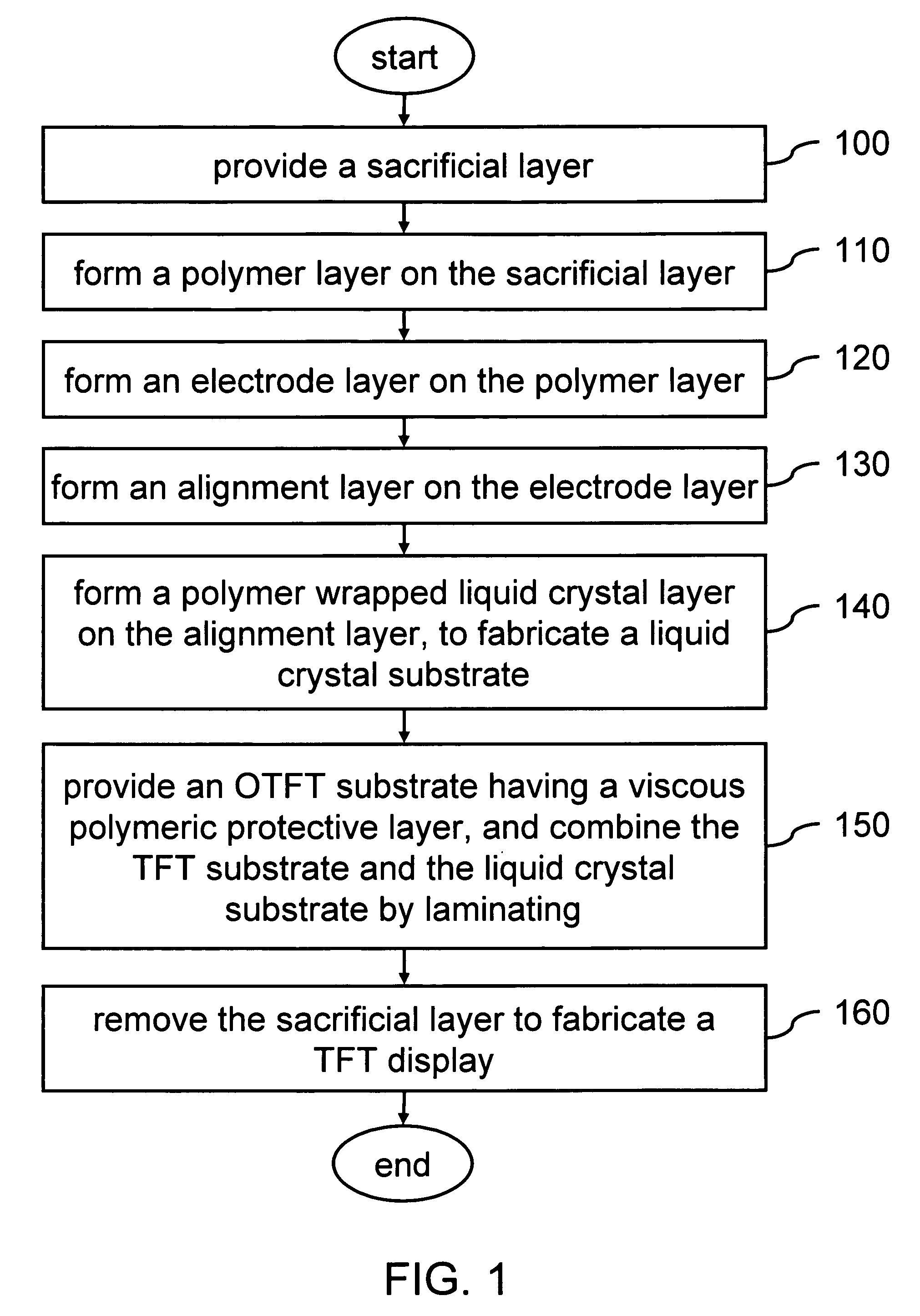
[0017] With reference to FIG. 1, the method for fabricating the OTFT primarily comprises the steps as follows:

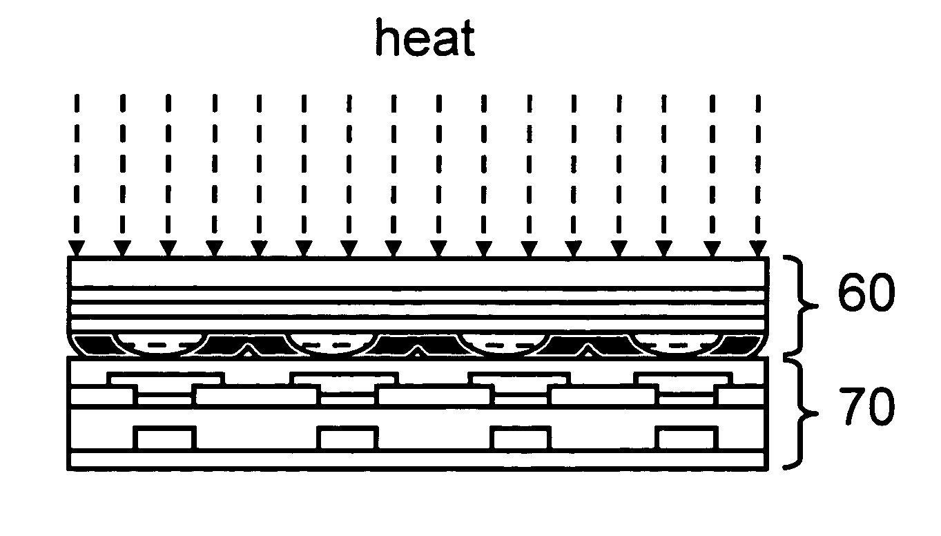
[0018] First, providing a sacrificial layer (step 100); then, forming a polymer layer on the sacrificial layer (step 110); and then forming an electrode layer on the polymer layer (step 120); afterwards, forming an alignment layer on the electrode layer (step 130); next, forming a polymer encapsulated liquid crystal layer on the alignment layer so as to fabricate a liquid crystal substrate (step 140); subsequently, providing an OTFT substrate having a adhesive polymeric protective layer, and combining the TFT substrate and the liquid crystal substrate by laminating (step 150); finally, removing the sacrificial layer, and the TFT display is fabricated (step 160).

[0019] Wherein, the TFT substrate employed in the invention is made of TFT selected from the group consisting of organic, inorganic TFT materials or a mixture of both. Taking only the OTFT for example hereinafter, a...


PUM

PropertyMeasurementUnit
thicknessaaaaaaaaaa
thicknessaaaaaaaaaa
thicknessaaaaaaaaaa

Abstract

A method for fabricating a thin film transistor (TFT) display is provided, wherein the processes of a liquid crystal substrate and an organic thin film transistor (OTFT) substrate are separated. The fabrication of liquid crystal substrate employs the technology of polymer encapsulated liquid crystal molecule, and leaves the polymeric layer as a substrate using a sacrificial layer, so as to improve the flexibility. And the TFT substrate has a high adhesive polymeric protective layer provided on its surface, so as to combine the fabricated TFT substrate and the liquid crystal substrate by laminating. Thereby, the processes of the liquid crystal substrate and the TFT substrate will not affect each other, to improve the process yield and meet the demand for the variety of products.

Description

BACKGROUND [0001] 1. Field of Invention [0002] The present invention relates to a method for fabricating a thin film transistor (TFT) display, in particular, to a method for fabricating a TFT display wherein the display section and TFT section are recombined after being processed separately, thereby improving the process yield. [0003] 2. Related Art [0004] In recent years, flexible flat panel display has the advantages such as low power consumption and high image quality, therefore it soon becomes the focus product since it came into the market. At the same time, based on the market demands for accommodation, portability and convenience, efforts have been exerted to develop flexible liquid crystal display (Flexi LCD) by those skilled in the art around the world, and many big companies have joined in this “display revolution” one after another. Organic thin film transistor (OTFT) makes use of organic molecule materials to develop TFTs adapted for electronic products. The transistor e...

Claims


Application Information

Patent Timeline
Patent Type & Authority Applications(United States)
IPC IPC(8): H01L21/84
CPCG02F1/1334G02F1/1341H01L51/107H01L51/0545G02F1/1362H10K10/88H10K10/466
Inventor HUANG, LIANG-YINHO, JIA-CHONGLEE, CHENG-CHUNGLIAO, CHI-CHANG
Owner IND TECH RES INST
Why Eureka
Try Eureka